Photovoltaic effect and its varieties
For the first time, the so-called photovoltaic (or photovoltaic) effect was observed in 1839 by the French physicist Alexandre Edmond Becquerel.
Experimenting in his father's laboratory, he discovered that by illuminating platinum plates immersed in an electrolytic solution, a galvanometer connected to the plates indicated the presence of electromotive force… Soon the nineteen-year-old Edmund found a useful application for his discovery — he created an actinograph — a device for recording the intensity of incident light.
Today, photovoltaic effects include a whole group of phenomena, in one way or another, related to the appearance of an electric current in a closed circuit, which includes an illuminated semiconductor or dielectric sample, or the EMF phenomenon on an illuminated sample, if the external circuit is open. In this case, two types of photovoltaic effects are distinguished.
The first type of photovoltaic effects include: high electric photo-EMF, volume photo-EMF, valve photo-EMF, as well as the photoepizoelectric effect and the Dember effect.
Photovoltaic effects of the second type include: the effect of entrainment of electrons by photons, as well as surface, circular and linear photovoltaic effects.
Effects of the first and second type
Photovoltaic effects of the first type are caused by a process in which a light effect generates mobile electric charge carriers of two characters — electrons and holes, which leads to their separation in the space of the sample.
The possibility of separation is related in this case either to the inhomogeneity of the sample (its surface can be considered as the inhomogeneity of the sample) or to the inhomogeneity of the illumination when light is absorbed close to the surface or when only part of the sample surface is illuminated , so the EMF arises due to an increase in the speed of thermal movement of electrons under the influence of light falling on them.
Photovoltaic effects of the second type are associated with the asymmetry of the elementary processes of excitation of charge carriers by light, the asymmetry of their scattering and recombination.
Effects of this type appear without the additional formation of pairs of opposite charge carriers, they are caused by interband transitions or can be related to the excitation of charge carriers by impurities, in addition, they can be caused by the absorption of light energy by the free charge carriers.
Next, let's look at the mechanisms of photovoltaic effects. We will first look at photovoltaic effects of the first type, then turn our attention to the effects of the second type.
Thicker effect
The Dember effect can occur under uniform illumination of the sample, simply because of the difference in surface recombination rates on its opposite sides. With uneven illumination of the sample, the Dember effect is caused by the difference in the diffusion coefficients (difference in mobility) of electrons and holes.
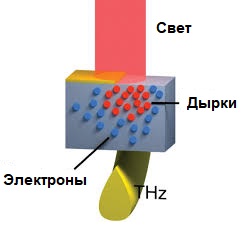
The Dember effect, initiated by pulsed illumination, is used to generate radiation in the terahertz range. The Dember effect is most pronounced in high-electron-mobility, narrow-gap semiconductors such as InSb and InAs.[banner_adsense]
Barrier photo-EMF
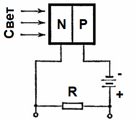
The gate or barrier photo-EMF results from the separation of electrons and holes by an electric field of the Schottky barrier in the case of a metal-semiconductor contact, as well as the field p-n-junction or heterojunction.
The current here is formed by the movement of both charge carriers directly generated in the region of the pn-junction, and those carriers that are excited in the regions close to the electrode and reach the region of the strong field by diffusion.
Pair separation promotes the formation of hole flow in the p region and electron flow in the n region. If the circuit is open, then the EMF acts in the direct direction for the p-n junction, so its action compensates for the original phenomenon.
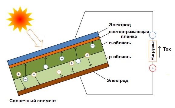
This effect is the basis of functioning solar cells and highly sensitive radiation detectors with low response.
Volumetric photo-EMF
Bulk photo-EMF, as its name suggests, arises as a result of the separation of pairs of charge carriers in the bulk of the sample at inhomogeneities associated with a change in the concentration of the dopant or with a change in the chemical composition (if the semiconductor is compound).
Here, the reason for the separation of the pairs is the so-called A counter electric field created by a change in the position of the Fermi level, which in turn depends on the impurity concentration. Or, if we are talking about a semiconductor with a complex chemical composition, the splitting of pairs results from a change in band width.
The phenomenon of the appearance of bulk photoelectrics is applicable to the probing of semiconductors to determine the degree of their homogeneity. The sample resistance is also related to inhomogeneities.
High voltage photo-EMF
Abnormal (high voltage) photo-EMF occurs when non-uniform illumination causes an electric field directed along the surface of the sample. The magnitude of the resulting EMF will be proportional to the length of the illuminated area and may reach 1000 volts or more.
The mechanism can be caused either by the Dember effect, if the diffuse current has a surface-directed component, or by the formation of a p-n-p-n-p structure projecting to the surface. The resulting high-voltage EMF is the total EMF of each pair of asymmetric n-p and p-n junctions.
Photoepizoelectric effect
The photoepizoelectric effect is the phenomenon of the appearance of a photocurrent or photoemf during deformation of the sample. One of its mechanisms is the appearance of bulk EMF during inhomogeneous deformation, leading to a change in the parameters of the semiconductor.
Another mechanism for the appearance of photoepisoelectric EMF is the transverse Dember EMF, which occurs under uniaxial deformation, which causes anisotropy of the diffusion coefficient of charge carriers.
The latter mechanism is most effective in multivalley semiconductor deformations, leading to a redistribution of carriers between valleys.
We have looked at all the photovoltaic effects of the first type, then we will look at the effects attributed to the second type.
The effect of electron attraction by photons
This effect is related to the asymmetry in the distribution of photoelectrons over the momentum obtained from the photons. In two-dimensional structures with optical miniband transitions, the sliding photocurrent is mainly caused by electron transitions with a certain momentum direction and can significantly exceed the corresponding current in bulk crystals.
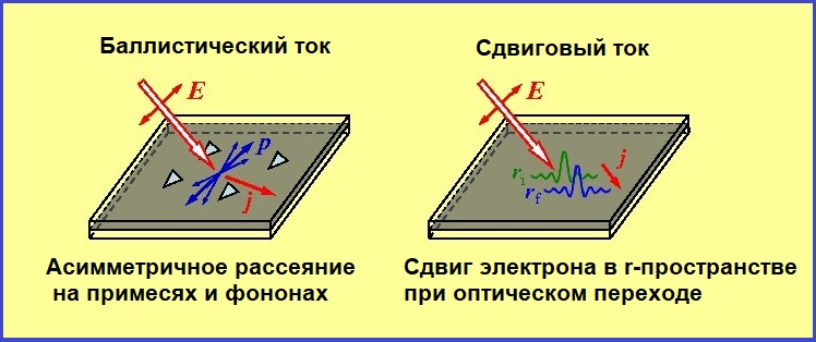
Linear photovoltaic effect
This effect is due to the asymmetric distribution of photoelectrons in the sample. Here, the asymmetry is formed by two mechanisms, the first of which is ballistic, related to the directionality of the pulse during the quantum transitions, and the second is shear, due to the shift of the center of gravity of the wavepacket of electrons during the quantum transitions.
The linear photovoltaic effect is not related to the transfer of momentum from photons to electrons, therefore, with a fixed linear polarization, it does not change when the direction of light propagation is reversed. The processes of light absorption and scattering and recombination contribute to the current (these contributions are compensated at thermal equilibrium).
This effect, applied to dielectrics, makes it possible to apply the mechanism of optical memory, because it leads to a change in the refractive index, which depends on the intensity of the light, and continues even after it is turned off.
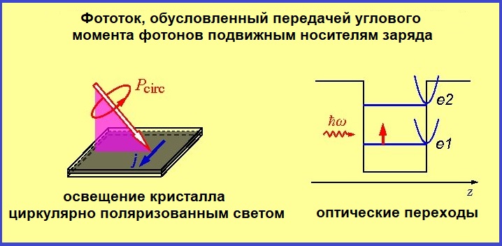
Circular photovoltaic effect
The effect occurs when illuminated by elliptically or circularly polarized light from gyrotropic crystals. The EMF reverses sign when the polarization changes. The reason for the effect lies in the relationship between spin and electron momentum, which is inherent in gyrotropic crystals. When electrons are excited by circularly polarized light, their spins are optically oriented, and accordingly a directional current pulse occurs.
The presence of the opposite effect is expressed in the appearance of optical activity under the action of a current: the transmitted current causes the orientation of the spins in gyrotropic crystals.
The last three effects serve in inertial receivers. laser radiation.
Surface photovoltaic effect
The surface photovoltaic effect occurs when light is reflected or absorbed by free charge carriers in metals and semiconductors due to the transfer of momentum from photons to electrons during oblique incidence of light and also during normal incidence if the normal to the surface of the crystal differs in direction from one of the principal crystal axes.
The effect consists in the phenomenon of scattering of light-excited charge carriers on the surface of the sample. In the case of interband absorption, it occurs under the condition that a significant fraction of the excited carriers reach the surface without scattering.
So when the electrons are reflected from the surface, a ballistic current is formed, directed perpendicular to the surface. If, upon excitation, the electrons arrange themselves in inertia, a current directed along the surface may appear.
The condition for the occurrence of this effect is the difference in the sign of the non-zero components of the average values of momentum "toward the surface" and "from the surface" for electrons moving along the surface. The condition is fulfilled, for example, in cubic crystals, upon excitation of charge carriers from the degenerate valence band to the conduction band.
In diffuse scattering by a surface, electrons reaching it lose the component of momentum along the surface, while electrons moving away from the surface retain it. This leads to the appearance of a current on the surface.