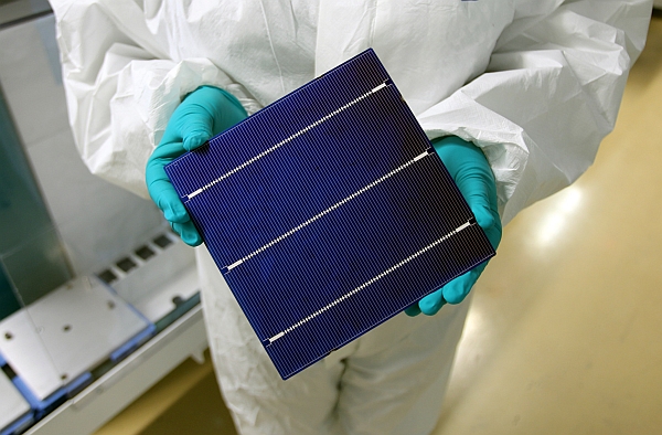
Production of photovoltaic cells for solar panels
The basis of any photovoltaic installation is always a photovoltaic module. A photovoltaic module is a combination of photovoltaic cells electrically connected together. The term photovoltaic consists of two words «photo» (from Greek. Light) and «volt» (Alessandro Volta - 1745-1827, Italian physicist) - a unit of measurement for voltage in electrical engineering. Analyzing the term photovoltaic, we can say — it is converting light into electricity.
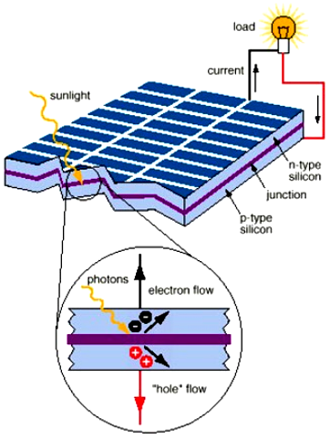
A photovoltaic cell (solar cell) is used to generate electricity by converting solar radiation. A photocell can be thought of as a diode made up of n-type and p-type semiconductors with a carrier-depleted region formed, so an unilluminated photocell is like a diode and can be described as a diode.
For semiconductors with a width between 1 and 3 eV, the maximum theoretical efficiency can be reached to 30%. The band gap is the minimum photon energy that can lift an electron from the valence band to the conduction band. The most common commercial solar cells are flint elements.
Silicon monocrystals and polycrystals. Silicon is today one of the most common elements for the production of photovoltaic modules. However, due to the low absorption of solar radiation, silicon crystal solar cells are usually made 300 µm wide. The efficiency of the silicon monocrystalline photocell reaches 17%.
If we take a polycrystalline silicon photocell, then the efficiency for it is 5% lower than that of monocrystalline silicon. The grain boundary of a polycrystal is the recombination center of charge carriers. The size of polycrystalline silicon crystals can vary from a few mm to one cm.
Gallium arsenide (GaAs). Gallium arsenide solar cells have already demonstrated an efficiency of 25% in laboratory conditions. Gallium arsenide, developed for optoelectronics, is difficult to produce in large quantities and quite expensive for solar cells. Gallium arsenide solar cells are applied along with solar concentrators, as well as for cosmonautics.
Thin film photocell technology. The main disadvantage of silicon cells is their high cost. Thin-film cells made of amorphous silicon (a-Si), cadmium telluride (CdTe) or copper-indium diselinide (CuInSe2) are available. The advantage of thin film solar cells is the saving of raw materials and cheaper production compared to silicon solar cells. Therefore, we can say that thin-film products have prospects for use in photocells.
The downside is that some materials are quite toxic, so product safety and recycling play an important role. In addition, telluride is a depleting resource compared to silicon.The efficiency of thin-film photocells reaches 11% (CuInSe2).
In the early 1960s, solar cells cost approximately $1,000/W peak power and were mostly manufactured in space. In the 1970s, mass production of photocells began and their price dropped to $100/W. Further progress and a reduction in the price of photocells made it possible to use photocells for household needs. Especially for part of the population living far from power lines and standard power supplies, photovoltaic modules have become a good alternative.
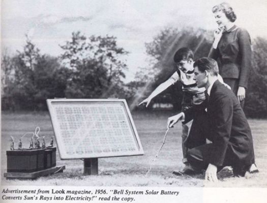
The photo shows the first silicon-based solar cell. It was created by scientists and engineers of the American company Bell Laboratories in 1956. A solar cell is a combination of photovoltaic modules electrically connected to each other. The combination is selected depending on the required electrical parameters such as current and voltage. One cell of such a solar battery, producing less than 1 watt of electricity, costs $250. The electricity produced was 100 times more expensive than from the conventional grid.
For almost 20 years, solar panels have only been used for space. In 1977, the cost of electricity was reduced to $76 per watt cell. Efficiency gradually increased: 15% in the mid-1990s and 20% by 2000. The current most relevant data on this topic —Efficiency of solar cells and modules
The production of silicon solar cells can be roughly divided into three main stages:
-
production of high purity silicon;
-
making thin silicone washers;
-
installation of the photocell.
The main raw material for the production of high purity silicon is quartz sand (SiO2)2). The melt is obtained by electrolysis metallurgical siliconwhich has a purity of up to 98%. The silicon recovery process takes place when sand interacts with carbon at a high temperature of 1800°C:
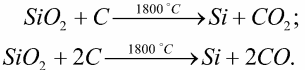
This degree of purity is not sufficient for the production of a photocell, so it must be further processed. The further purification of silicon for the semiconductor industry is carried out practically all over the world using technology developed by Siemens.
«Siemens Process» is the purification of silicon by the reaction of metallurgical silicon with hydrochloric acid, resulting in trichlorosilane (SiHCl3):
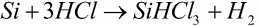
Trichlorosilane (SiHCl3) is in the liquid phase, so it is easily separated from the hydrogen. In addition, repeated distillation of trichlorosilane increases its purity to 10-10%.
The subsequent process — pyrolysis of purified trichlorosilane — is used to produce high-purity polycrystalline silicon. The resulting polycrystalline silicon does not fully meet the conditions for use in the semiconductor industry, but for the solar photovoltaic industry, the quality of the material is sufficient.
Polycrystalline silicon is a raw material for the production of monocrystalline silicon. Two methods are used for the production of monocrystalline silicon — the Czochralski method and the zone melting method.
Czochralski's method is energy intensive as well as material intensive. A relatively small amount of polycrystalline silicon is charged into the crucible and melted under vacuum.A small seed of monosilicon falls on the surface of the melt and then, twisting, rises, pulling the cylindrical ingot behind it, due to the force of surface tension.
At present, the diameters of the drawn ingots are up to 300 mm. The length of the ingots with a diameter of 100-150 mm reaches 75-100 cm. The crystal structure of the elongated ingot repeats the monocrystalline structure of the seed. Increasing the diameter and length of an ingot, as well as improving the technology of its cutting, will reduce the amount of waste, thus reducing the cost of the resulting photocells.
Belt technology. The technological process developed by Mobil Solar Energy Corporation is based on pulling silicon strips from the melt and forming solar cells on them. The matrix is partially immersed in the silicon melt and, due to the capillary effect, the polycrystalline silicon rises, forming a ribbon. The melt crystallizes and is removed from the matrix. In order to increase productivity, the equipment is designed, on which it is possible to receive up to nine belts at the same time. The result is a nine-sided prism.
The advantage of belts is that they are low-cost due to the fact that the process of cutting the ingot is excluded. In addition, rectangular photovoltaic cells can be easily obtained, while the round shape of monocrystalline plates does not contribute to the good placement of the photovoltaic cell in the photovoltaic module.
The resulting polycrystalline or monocrystalline silicon rods must then be cut into thin wafers 0.2-0.4 mm thick. When cutting a rod of monocrystalline silicon, about 50% of the material is lost in losses.Also, round washers are not always, but often, cut to make a square shape.