I2C bus — assignment, device, data transfer, addressing
When creating an electronic circuit, many developers are faced with the need to use a large number of intermediate chips for matching, sampling and addressing its individual blocks. To minimize the number of auxiliary chips, Philips proposed a two-wire bidirectional I2C serial network interface back in the 1980s, designed specifically to manage multiple chips within a single device.
Today, Philips alone produces more than a hundred I2C-compatible devices for electronic equipment with a wide variety of purposes: memory, video processor systems, analog-to-digital and digital-to-analog converters, display drivers, etc.
The I2C bus is a modification of the serial data exchange protocol capable of transmitting serial 8-bit data in the usual "fast" mode at rates of 100 to 400 kbps. The process of data exchange is implemented here on only two wires (not counting the common wire): SDA line for data and SCL line for synchronization.
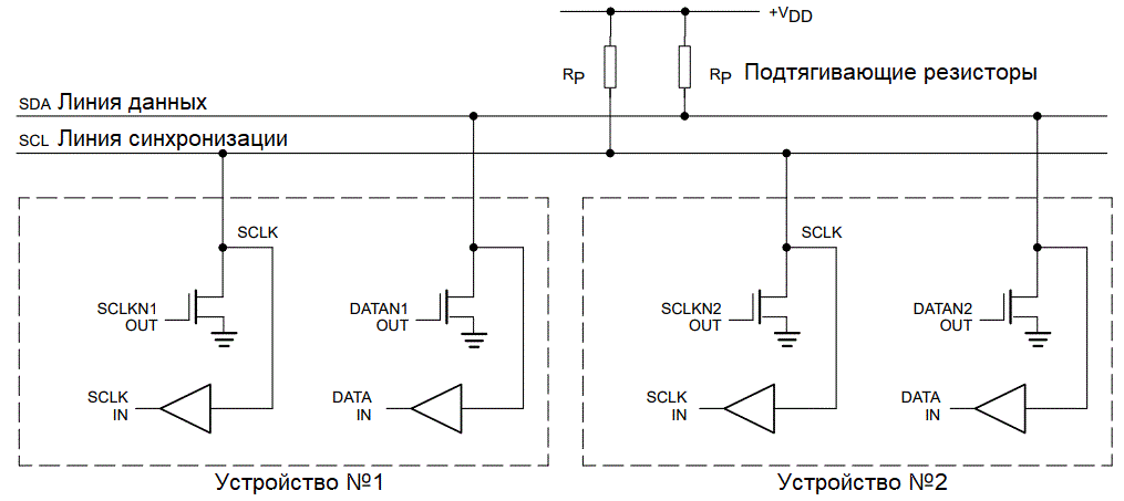
The bus becomes bi-directional due to the fact that the cascades of outputs of devices connected to the bus have open collectors or channels, thus replicating the AND wiring. As a result, the bus minimizes the number of connections between chips, leaving fewer required pins and traces on the board. As a result, the board itself turns out to be simpler, more compact and technologically more advanced in production.
This protocol allows you to disable address decoders and other external negotiation logic. The number of chips that can operate simultaneously on the I2C bus is limited by its capacity — a maximum of 400 pF.
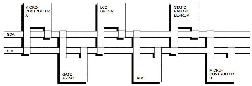
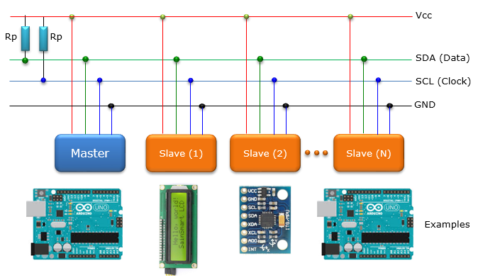
I2C-compatible ICs have a hardware noise suppression algorithm to ensure data integrity even in the presence of strong interference. Such devices have an interface that allows the microcircuits to communicate with each other even when their supply voltages are different. In the figure below, you can familiarize yourself with the principle of connecting several microcircuits through a common bus.
Each of the devices connected to the bus has its own unique address, it is determined by it and, in accordance with the purpose of the device, it can work as a receiver or as a transmitter. When transmitting data, these devices can be master (master) or slave (slave). The master is the device that initiates the data transfer and generates clock signals on the SCL line. The slave, in relation to the master, is the destination device.
At any given moment of operation on the I2C bus, only one device can act as a master; it generates a signal on the SCL line.A master can be either a master receiver or a master transmitter.
In principle, the bus allows several different masters, but imposes restrictions on the characteristics of forming control signals and monitoring the status of the bus; this means that several masters can start transmitting at the same time, but conflicts of this kind are eliminated thanks to arbitration, that is, the way the master behaves when it detects that the bus is occupied by another master.
Synchronization of a pair of devices is ensured by the fact that all devices are connected to the bus, forming an "AND" wiring. Initially, the SDA and SCL signals are high.
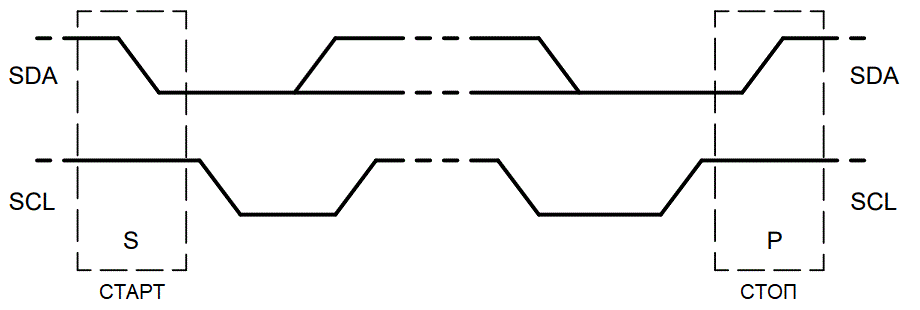
START and STOP
The exchange starts with the master generating the «START» state: on the SDA line, the signal goes from high to low state, while the SCL line has a stable high level. All devices connected to the bus perceive this situation as a command to start the exchange.
Each master generates an individual clock signal on the SCL line when transmitting data on the bus.
The exchange ends with the formation of the STOP state by the master: on the SDA line the signal changes from low to high, while the SCL line has a stable high level.
The driver always acts as the source of the START and STOP signals. As soon as the «START» signal is fixed, it means that the line is busy. The line is free when a STOP signal is detected.
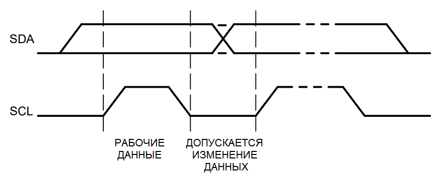
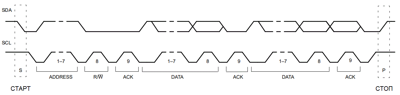
Immediately after declaring the START state, the master switches the SCL line low and sends the most significant bit of the first message byte to the SDA line. The number of bytes in a message is not limited.Changes on the SDA line are enabled only when the signal level on the SCL line is low. The data is valid and should not be changed only when the sync pulse is high.
Acknowledgment that the byte from the master transmitter has been received by the slave receiver is done by setting a special acknowledge bit on the SDA line after the eighth data bit has been received.
THE CONFIRMATION
So, sending 8 bits of data from the transmitter to the receiver ends up with an extra pulse on the SCL line when the receiving device goes low on the SDA line, indicating that it has received the entire byte.
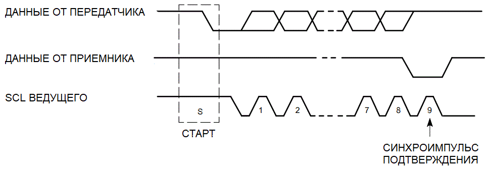
Confirmation is an integral part of the data transfer process. The master generates a sync pulse. The transmitter sends a low state to SDA while the acknowledge clock is active. While the sync pulse is high, the receiver must keep SDA low.
If the destination slave does not acknowledge its address, for example because it is currently busy, the data line must be held high. The master may then give a STOP signal to abort the dispatch.
If the reception is carried out by the master receiver, then it is obliged to inform the slave transmitter after the completion of the transmission - not by confirming the last byte. The slave transmitter releases the data line so that the master can issue a STOP signal or a repeating START signal.
The synchronization of the devices is ensured by the fact that the connections to the SCL line are made according to the "AND" principle.
The master does not have the sole right to control the transition of the SCL line from low to high.If the slave needs more time to process a received bit, it can independently hold SCL low until it is ready to receive the next bit of data. The SCL line in such a situation will be low for the duration of the longest low-level sync pulse.
Devices with the lowest sustained low will remain idle until the long period ends. When all devices have finished the low sync period, SCL will go high.
All devices will start clocking high and the first device to complete its period will be the first to set the SCL line low. As a result, the duration of the low state of SCL will be determined by the longest low state of the synchronization pulse of one of the devices, and the duration of the high state will be determined by the shortest period of synchronization of one of the devices.
Synchronization signals can be used by receivers as a means of controlling data transmission at the bit and byte level.
If the device is capable of receiving bytes at a high rate, but it takes a certain amount of time to store the received byte or prepare to receive the next byte, it may continue to hold SCL low after receiving and acknowledging a byte , forcing the transmitter into a standby state.
A microcontroller without built-in hardware circuits, for example at the bit level, can slow down the clock speed by increasing the duration of their low state. As a result, the baud rate of the master device will be determined by the speed of the slower device.
ADDRESSING
Each device connected to the I2C bus has a unique program address at which the master addresses it by sending a specific command. Microcircuits of the same type are characterized by an address selector, implemented either in the form of digital inputs of the selector, or in analog form. Addresses are divided into the address space of the devices connected to the bus.
Normal mode assumes seven-bit addressing. Addressing works as follows: after the «START» command, the master sends the first byte, which determines which slave device is needed to communicate with the master. There is also a common call address that defines all devices on the bus, all devices (theoretically) respond to it with an acknowledgment, but in practice this is rare.
So the first seven bits of the first byte are the slave address. The least significant bit, the eighth, indicates the direction of sending data. If there is a «0», then the information will be written from the master to this slave. If «1», the information will be read by the master from this slave.
After the master finishes sending the address byte, each slave compares its address to it. Anyone with the same address is a slave and is defined as a slave transmitter or slave receiver, depending on the value of the least significant bit of the address byte.
A slave address can include fixed and programmable parts. Quite often a large number of devices of the same type work in one system, then the programmable part of the address allows the use of a maximum of the same type of devices on the bus. How many bits in the address byte are programmable depends on the number of free pins on the chip.
Sometimes a pin with an analog setting of the programmable address range is sufficient, for example the SAA1064 - an LED indicator driver that has exactly such an implementation. The potential of a particular pin determines the offset of the address space of the chip so that chips of the same type do not conflict operating on the same bus. All chips supporting the I2C bus contain a set of addresses that the manufacturer specifies in the documentation.
The combination «11110XX» is reserved for 10-bit addressing. If we imagine the exchange of data from the «START» command to the «STOP» command, it will look like this:
Simple and combined data exchange formats are allowed here. The combined format means that between «START» and «STOP» the master and slave can act as receivers and transmitters, this is useful for example in serial memory management.
Let the first byte of data transfer a memory address. Then, repeating the «START» command and reading the slave address, the memory data will work. Decisions to automatically increment or decrement the previously accessed address are made by the device developer after having previously studied the chip documentation. One way or another, after receiving the START command, all devices must restore their logic and prepare for the fact that the address will now be named.