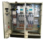
AC semiconductor devices
 The schematic diagram and design of AC semiconductor electrical devices are determined by the purpose, requirements and operating conditions. With the wide application that contactless devices find, there is a wide variety of possibilities for their implementation. However, all of them can be represented by a generalized block diagram that shows the required number of functional blocks and their interaction.
Figure 1 shows a block diagram of an AC semiconductor device in unipolar construction. It includes four functionally complete units.
The power supply unit 1 with surge protection elements (RC-circuit in Figure 1) is the basis of the switching device, its executive body. It can be done on the basis of only controlled valves - thyristors or with the help of diodes.
When designing a device for current exceeding the current limits of a single device, it is necessary to connect them in parallel.In this case, special measures must be taken to eliminate the uneven distribution of current in individual devices, which is due to the non-identity of their current-voltage characteristics in the conductive state and the distribution of the turn-on time.
Control block 2 contains devices that select and remember commands coming from the control or protection bodies, generate control pulses with set parameters, synchronize the arrival of these pulses at the thyristor inputs with the moments when the current in the load crosses zero.
The circuit of the control unit becomes much more complex if the device, in addition to the circuit switching function, has to regulate voltage and current. In this case, it is supplemented by a phase control device, which provides a shift of the control pulses by a given angle relative to the zero current.
The block of sensors for the operation mode of the apparatus 3 contains measuring devices for current and voltage, protective relays for various purposes, a circuit for generating logical commands and signaling the switching position of the apparatus.
The forced switching device 4 combines a capacitor bank, its charging circuit and switching thyristors. In alternating current machines, this device is contained only if they are used as protection (circuit breakers).
The power part of the device can be made according to a scheme with antiparallel connection of thyristors (see figure 1), based on a symmetrical thyristor (triac) (figure 2, a) and in various combinations of thyristors and diodes (figure 2, b and c ).
In each specific case, when choosing a circuit option, the following factors should be taken into account: the voltage and current parameters of the device being developed, the number of devices used, the long-term load carrying capacity and resistance to current overloads, the degree of complexity of the thyristor handling, weight and size requirements and cost.
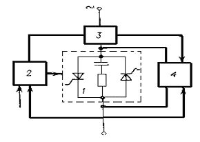
Figure 1 — Block diagram of an AC thyristor device
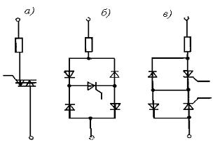
Figure 2 — Power blocks of AC semiconductor devices
A comparison of the power blocks shown in Figures 1 and 2 shows that the scheme with anti-parallel connected thyristors has the greatest advantages. Such a scheme contains fewer devices, has smaller dimensions, weight, energy loss and cost.
Compared to triacs, thyristors with unidirectional (one-way) conduction have higher current and voltage parameters and are able to withstand significantly greater current overloads.
Tablet thyristors have a higher thermal cycle. Therefore, a circuit using triacs can be recommended for switching currents that, as a rule, do not exceed the current rating of a single device, that is, when their group connection is not required. Note that the use of triacs helps to simplify the control system of the power supply unit, it must contain an output channel to the pole of the apparatus.
The schemes shown in figure 2, b, c illustrate the possibility of designing alternating current switching devices using diodes. Both schemes are easy to manage, but have disadvantages due to the use of a large number of devices.
In the circuit of Figure 2, b, the alternating voltage of the power source is converted to a full-wave voltage of one polarity using a diode bridge rectifier. As a result, only one thyristor connected at the output of the rectifier bridge (in the diagonal of the bridge) becomes capable of controlling the current in the load during the two half-cycles, if at the beginning of each half-cycle the control pulses are received at its input. The circuit is switched off at the nearest zero crossing of the load current after stopping the generation of control pulses.
It should be borne in mind, however, that reliable tripping of the circuit is ensured only with a minimum inductance of the circuit on the side of the rectified current. Otherwise, even if the voltage drops to zero at the end of the half-cycle, current will continue to flow through the thyristor, preventing it from turning off. The danger of emergency tripping of the circuit (without tripping) also occurs when the frequency of the supply voltage increases.
 In the circuit, in Figure 2, the load is controlled by two thyristors connected together, each of which is manipulated in the opposite direction by an uncontrolled valve. Since in such a connection the cathodes of the thyristors are at the same potential, this allows the use of single-output or two-output control pulse generators with a common ground.
The schematic diagrams of such generators are greatly simplified. In addition, the thyristors in the circuit, in Figure 2, c, are protected against reverse voltage and therefore should be selected only for forward voltage.
In terms of dimensions, technical characteristics and economic indicators, the devices made according to the schemes shown in Figure 2, b, c are inferior to the switching devices whose circuits are shown in Figures 1 c, 2, a. Nevertheless, they are widely used in automation and relay protection devices, where switching power is measured in hundreds of watts. In particular, they can be used as output devices of pulse shapers to control thyristor blocks of more powerful devices.
Timofeev A.S.