Digital devices: flip-flops, comparators and registers
 Digital devices are built on logical elements, therefore they obey the laws of logical algebra. The basic devices of digital technology, along with logic devices, are flip-flops.
Trigger (English trigger - trigger) - an electronic device that has two stable states and can jump from one state to another under the influence of an external impulse.
Triggers or, more precisely, trigger systems are called a large class of electronic devices that have the ability to remain in one of two stable states for a long time and alternate them under the influence of external signals. Each trigger condition is easily recognized by the output voltage value.
Each trigger state corresponds to a certain (high or low) output voltage level:
1) the trigger is set to one state — level «1».
2) the flip-flop is reset — level «0» at the output.
The steady state remains as long as desired and can be changed by an external pulse or by switching off the supply voltage. Che.a flip-flop is an elementary memory element capable of storing the smallest unit of information (one bit) «0» or «1».
Flip-flops can be built on discrete elements, logic elements, on an integrated circuit or are part of an integrated circuit.
The main types of flip-flops include: RS-, D-, T-, and JK-flippers... In addition, flip-flops are divided into asynchronous and synchronous. In asynchronous actuation, switching from one state to another is done directly with the arrival of a signal to the information input. In addition to data inputs, synchronized flip-flops have a clock input. Their switching takes place only in the presence of an enabling clock pulse.
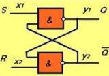
An RS trigger has at least two inputs: S (set — set) — the trigger is set to the state of level «1» and R (reset) — the trigger is reset to the state of level «0». (Fig. 1).
In the presence of input C, the flip-flop is synchronous — switching of the flip-flop (change of state of the output) can occur only at the moment of arrival of the synchronizing (synchronizing) pulse at input C.
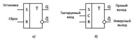
Figure 1 — Conventional graphical representation of the RS flip-flop and the purpose of conclusions a) asynchronous, b) synchronous
In addition to the direct output, the flip-flop can also have an inverse output, the signal of which will be opposite.
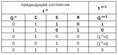
Table 1 shows the states that the flip-flop can assume during operation. The table shows the values of the input signals S and R at a certain instant of time tn and the state of the flip-flop (of the direct output) at the next instant of time tn + 1 after the arrival of the next pulses. The new trigger state is also affected by the previous state of Q n.
Che.if it is necessary to write to the trigger «1» — we give a pulse to the S input, if «0» — we send a pulse to the R input.
The combination S = 1, R = 1 is a forbidden combination because it is impossible to predict what state will be established at the output.
Table 1 - Synchronous RS flip-flop state table
The operation of the flip-flop can also be seen using timing diagrams (Fig. 2).
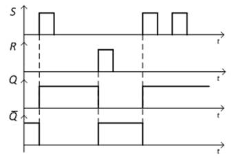
Figure 2 — Timing diagrams of an asynchronous RS flip-flop
D-trigger (from English delay — delay) has one information input and a clock (synchronizing) input (Fig. 3).
The D-flip-flop stores and stores at the output Q the signal that was at the data input D at the time of arrival of the clock pulse C. the flip-flop stores information written when C = 1.
Table 2-Table of states of the D-flip-flop
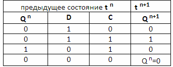
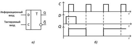
Figure 3 — D -trigger: a) conventional graphical representation, b) timing diagrams of operation
T-triggers (from the English tumble — overturning, somersault), also called counting flip-flops, have one information input T. Each pulse (pulse decay) of the T-input (counting input) switches the trigger to the opposite state.
Figure 4 shows the T-trigger symbology (a) and timing diagrams of operation (b).
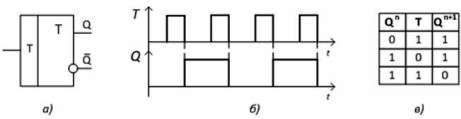
Figure 4-T-flip-flop a) conventional-graphic notation, b) timing diagrams of operation c) state table
A JK trigger (from the English jump — jump, keer — hold) has two data inputs J and K and a clock input C. The assignment of pins J and K is similar to the assignment of pins R and S, but the trigger has no prohibited combinations. If J = K = 1, it changes its state to the opposite (Fig. 5).
With appropriate connection of the inputs, the trigger can perform the functions of RS-, D-, T-triggers, i.e. is a universal trigger.
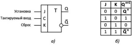
Figure 5 -JK -flip-flop a) conventional -graphic notation, b) abbreviated state table
Comparator (compare — compare) — a device that compares two voltages — input Uin with a reference Uref. The reference voltage is a constant voltage with positive or negative polarity, the input voltage changes over time. The simplest comparator circuit based on an operational amplifier is shown in Figure 6, a. If Uin Uop at the output U — us (Fig. 6, b).
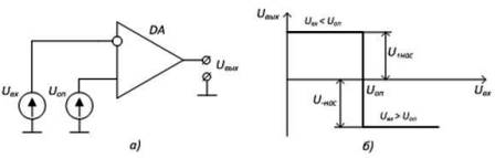
Figure 6 — Op-amp comparator: a) the simplest scheme b) performance characteristics
A positive feedback comparator is called a Schmitt trigger. If the comparator switches from «1» to «0» and vice versa at the same voltage, then the Schmitt trigger - at different voltages. The reference voltage creates a PIC circuit R1R2, the input signal is fed to the inverting input of the op-amp. Figure 7, b, shows the transfer characteristic of the Schmitt trigger.
At a negative voltage at the inventory input of the OS Uout = U + sat. This means that a positive voltage acts on the non-inverting input. As the input voltage increases, the current Uin > Uneinv. (Uav — trigger) the comparator goes to state Uout = U -sat. A negative voltage is applied to the non-inverting input. Accordingly, with a decrease in the input voltage at the moment Uin <Uneinv. (Uav — trigger) the comparator goes into state Uout = U + sat.
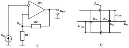
Figure 7 — Schmitt operation of an op-amp: a) the simplest scheme b) performance characteristics
An example. Figure 8 shows a schematic of a relay-contactor for controlling an electric motor, allowing it to start, stop and reverse.
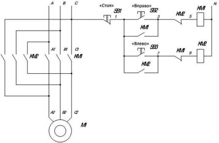
Figure 8 — Relay-contactor motor control scheme
The commutation of the electric motor is carried out by magnetic starters KM1, KM2. Freely closed contacts KM1, KM2 prevent the simultaneous operation of magnetic starters. Freely open contacts KM1, KM2 provide self-locking of buttons SB2 and SB3.
To improve the reliability of operation, it is necessary to replace the relay-contactor control circuits and power circuits with a non-contact system using semiconductor devices and devices.
Figure 9 shows a contactless motor control circuit.
The power contacts of the magnetic starters were replaced with opto-simistors: KM1-VS1-VS3, KM2-VS4-VS6. The use of optosimistors makes it possible to isolate a low-current control circuit from a powerful supply circuit.
Triggers provide self-locking buttons SB2, SB3. Logic elements AND ensure simultaneous activation of only one of the magnetic starters.
When the transistor VT1 opens, the current flows through the LEDs of the first group of opto-simistors VS1-VS3, thereby ensuring the flow of current through the motor windings. The opening of the transistor VT2 supplies the second group of opto-simistors VS4-VS6, ensuring the rotation of the electric motor in the other direction.
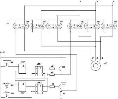
Figure 9 — Contactless motor control circuit
Register - an electronic device designed for short-term storage and conversion of multi-digit binary numbers. The register consists of flip-flops, the number of which determines how many bits of a binary number the register can store — the size of the register (Fig. 10, a). Logic elements can be used to organize the operation of triggers.
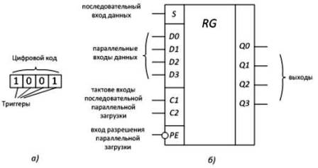
Figure 10 — Register: a) general representation, b) conventional graphical notation
According to the method of input and output of information, registers are divided into parallel and serial.
In a sequential register, the flip-flops are connected in series, that is, the outputs of the previous flip-flop pass information to the inputs of the next flip-flop. Flip-flop clock inputs C are connected in parallel. Such a register has one data input and a control input—clock input C.
A parallel register simultaneously writes to flip-flops for which there are four data inputs.
Figure 10 shows the UGO and the pin allocation of a four-bit parallel-serial register.