Printed circuit boards
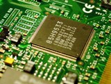 Printed circuit - an assembly block for electronic equipment in which the connecting wires of the circuit are applied to an insulating base (board) by a polygraphic method. To the ends of the printed circuit wires, wires or jumpers are soldered from the mounting wires connecting the printed wires to the hinged elements of the circuit.
The use of printed circuits repeatedly reduces the size of the equipment and radically changes the technology of its production (time-consuming manual assembly is eliminated, the number of soldered joints is reduced), makes it possible to automate production and increases the uniformity of products and its reliability.
The plate material must adhere well to the metal, have high mechanical strength, low shrinkage and retain its properties under the influence of climatic factors. Materials that partially meet the listed requirements include: high-frequency organic materials, getinax, materials based on phenol-formaldehyde resins, ceramics and glass.
The following methods of drawing an image are most often used:
-
typographical,
-
photochemical, using different light-sensitive emulsions,
-
application of wax mixtures and varnish films using a metal template,
-
offset printing.
The most productive are the photochemical method and offset printing, for which there is a well-developed technology for the production of printed circuit boards.
Depending on the material, printed circuit boards are produced by the following methods:
-
by etching a foil-coated dielectric;
-
foil stamping, with the diagram cut out and simultaneously glued to the plate;
-
applying a silver pattern by stencil on a plate of ceramic, mica, glass, followed by burning in silver;
-
applying a circuit to a plate by electrochemical copper deposition, pressing into wires, transferring an electroplated printed circuit from a die to a substrate.
The following methods are used for soldering the wires of radio components or assembly wires with current-carrying wires of the printed circuit: conventional using an electric soldering iron, mechanized with preliminary manual fixation of the wires of parts in the holes of a printed board and subsequent soldering of the connection points by immersion in molten solder (these methods, due to their low productivity, are mainly used in small-scale and pilot production).
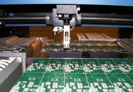
In mass and large-scale production, parts are mounted on a plate on an automatic line, followed by soldering of the contact points by immersion in molten solder.
To protect the printed wiring boards from mechanical and climatic factors, a layer is applied to them by a spraying method, followed by drying in air or in a thermostat. insulating varnish.
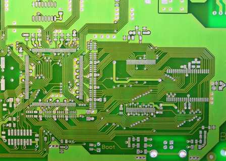
The printed circuit leads are located on one or both sides of the board. One-sided circuit arrangement greatly complicates the design task, but provides technological and economic advantages (for example, the possibility of immersion soldering).
Single sided stacking is widely used for relatively simple printed circuits. It is recommended to use two-sided wire arrangement for complex circuits that require a large number of jumpers for one-sided arrangement of wires, and in the case of a two-layer or multi-layer assembly structure, when it is necessary to connect the wires of the plates and the wires of parts located on different plates, between them, as well as in the design of ultra-miniature compact equipment.
When placing parts on a plate, they strive to ensure the minimum length of wires and a minimum of their intersections. In double-sided installation, the cross wires are placed on opposite sides of the insulating plate.
On one side of the board, the other printed leads are transferred using a metal layer that is deposited on the walls of the holes at the same time as the leads are applied.
The thickness and width of the printed wire are selected depending on its material, current density, transmitted power, permissible voltage drop, the required mechanical strength of the connection with the insulating plate and the technology of applying wires. In practice, the width of the printed wire is from 1 to 4 mm.
Increased heating of the printed wire can cause the plate to peel off and then break.To prevent swelling and peeling (for example, when using getinax), slot-like windows or windows in the form of etched areas are made in some parts of the circuit.
The distances between the printed wires are set depending on the allowable voltages. The minimum permissible distance between the edges of the wires is 1.0 — 1.5 mm.
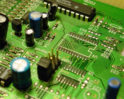
The printed wires are connected to the terminals of the hinged electronic elements (resistors, capacitors, etc.) and assembly jumpers by soldering with POS-60 solder. In places of soldering, the printed wire expands to some extent and covers the hole, the inner surface of which is also metallized and forms a single unit with the wire.
For the most complete filling of the holes with solder, their diameter should be 0.5 mm larger than the diameter of the connector, wire or outlet of the radio component. Increasing the extended portion of the printed wire leads to an increase in the strength of its connection to the plate. Often, to strengthen the connection of the wires to the plate at the ends, it will connect, the wires of the circuit are expanded with hollow metal caps.
Mechanized and automated assembly and assembly of printed circuit boards is possible only with a one-sided arrangement of parts, when on one side of the board there are all hinged elements (including various jumpers and assemblies), and on the other - all printed wires and their soldered connections with hinged elements .
Automating hardware assembly using printed circuit boards is largely dependent on the wiring design of the parts.For manufacturability reasons, the best terminal design is considered to be a round wire that is easy to manufacture and bend into a ring or other shape.
Printed wiring technology requires the use of a unified standard design and dimensions of electronic parts and circuit elements. Most often, printed circuits are used in the production of devices and units with a relatively complex design.
The widespread introduction of printed circuits radically changes the technological process of manufacturing electronic equipment towards its partial and full automation.
Inductors are applied to the surface of the insulating base in the form of a spiral radiating from the center. Their quality (dignity) is mainly determined by the thickness of the layer of the conductive pattern and the material of the plate. Permanent printed resistances are obtained by applying a rectangular pattern of graphite slurry with carbon black on the insulating substrate.
Permanent capacitors of relatively small size are obtained by depositing a metallized layer on two mutually opposite sides of the insulating base, which serves as plates. Work is also underway to master and introduce printed multi-turn coils, printed transformers, and other complex circuit elements.
Printed circuits are widely used in industrial electronics equipment, in various amplifier circuits, radio equipment, in computing equipment and other devices manufactured in large quantities.