Parameters of field-effect transistors: what is written in the data sheet
 Power inverters and many other electronic devices today rarely do without the use of powerful MOSFETs (field effect) or IGBT transistors… This applies both to high-frequency converters such as welding inverters, and to various home projects, the schematics of which are full on the Internet.
The parameters of currently produced power semiconductors allow switching currents of tens and hundreds of amperes at voltages up to 1000 volts. The choice of these components on the modern electronics market is quite wide, and choosing a field-effect transistor with the necessary parameters is by no means a problem today, since every self-respecting manufacturer accompanies a specific model of a field-effect transistor with technical documentation, which can always be found both on the manufacturer's official website and at official dealers.
Before proceeding with the design of this or that device using the specified power supply components, you should always know what exactly you are dealing with, especially when choosing a specific field-effect transistor.For this purpose, they turn to information sheets. A data sheet is an official document from an electronic component manufacturer that contains descriptions, parameters, product features, typical diagrams, and more.
Let's see what parameters the manufacturer indicates in the data sheet, what they mean and what they are for. Let's look at an example data sheet for an IRFP460LC FET. This is a fairly popular HEXFET power transistor.
HEXFET implies such a crystal structure where thousands of parallel-connected hexagonal MOSFET cells are organized into a single crystal. This solution made it possible to significantly reduce the resistance of the open channel Rds (on) and made it possible to switch large currents. However, let's move on to reviewing the parameters listed directly in the data sheet of the IRFP460LC from the International Rectifier (IR).
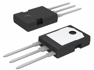
See Fig_IRFP460LC
At the very beginning of the document, a schematic image of the transistor is given, the designations of its electrodes are given: G-gate (gate), D-drain (drain), S-source (source), and also its main parameters are indicated and are distinguished qualities listed. In this case, we see that this N-channel FET is designed for a maximum voltage of 500 V, its open channel resistance is 0.27 Ohm, and its limiting current is 20 A. The reduced gate charge allows this component to be used in high frequency circuits at low energy costs for switching control. Below is a table (Fig. 1) with the maximum permissible values of various parameters in various modes.
-
Id @ Tc = 25 °C; Continuous Drain Current Vgs @ 10V — The maximum continuous, continuous drain current, at a FET body temperature of 25 °C, is 20 A. At a gate-source voltage of 10 V.
-
Id @ Tc = 100 °C; Continuous Drain Current Vgs @ 10V — The maximum continuous, continuous drain current, at a FET body temperature of 100 °C, is 12 A. At a gate-source voltage of 10 V.
-
Idm @ Tc = 25 °C; Pulse Drain Current — The maximum pulse, short-term drain current, at a FET body temperature of 25 °C is 80 A. Subject to an acceptable junction temperature. Figure 11 (Figure 11) provides an explanation of the relevant relationships.
-
Pd @ Tc = 25 °C Power Dissipation — The maximum power dissipated by the transistor case, at a case temperature of 25 °C, is 280 W.
-
Linear Derating Factor — For every 1°C increase in case temperature, power dissipation increases by an additional 2.2 watts.
-
Vgs Gate-to-Source Voltage - The maximum gate-to-source voltage should not be higher than +30V or below -30V.
-
Eas Single Pulse Avalanche Energy — The maximum energy of a single pulse in the sewer is 960 mJ. An explanation is given in fig. 12 (Fig. 12).
-
Iar Avalanche Current — The maximum interrupting current is 20 A.
-
Ear Repetitive Avalanche Energy — The maximum energy of repeated pulses in the sewer shall not exceed 28 mJ (for each pulse).
-
dv / dt Peak Diode Recovery dv / dt — The maximum rate of rise of the drain voltage is 3.5 V / ns.
-
Tj, Tstg Temperature range of junction operation and storage — Safe temperature range from -55 ° C to + 150 ° C.
-
Soldering temperature, for 10 seconds — the maximum soldering temperature is 300 ° C, and at a distance of at least 1.6 mm from the body.
-
Mounting torque, 6-32 or M3 screw — maximum housing mounting torque should not exceed 1.1 Nm.
Below is a table of temperature resistances (Fig. 2.). These parameters will be necessary when choosing a suitable radiator.
-
Rjc junction to case (crystal case) 0.45 ° C / W.
-
Rcs Body to sink, flat, lubricated surface 0.24 ° C / W
-
Rja Junction-to-Ambient depends on the heatsink and ambient conditions.
The following table contains all the necessary electrical characteristics of the FET at a die temperature of 25 ° C (see Fig. 3).
-
V (br) dss Source-to-source output voltage—the source-to-source voltage at which breakdown occurs is 500 V.
-
ΔV (br) dss / ΔTj Breakdown voltage temperature. Coefficient — temperature coefficient, breakdown voltage, in this case 0.59 V / ° C.
-
Rds (on) Static resistance between source and source - the resistance between source and source of the open channel at a temperature of 25 ° C, in this case it is 0.27 Ohm. It depends on the temperature, but more on that later.
-
Vgs (th) Gres Threshold Voltage — the threshold voltage for switching on the transistor. If the gate-source voltage is less (in this case 2 — 4 V), then the transistor will remain closed.
-
gfs Forward Conductance — The slope of the transfer characteristic equal to the ratio of the change in drain current to the change in gate voltage. In this case, it is measured at a drain-source voltage of 50 V and a drain current of 20 A. Measured in Amps / Volts or Siemens.
-
Idss Source-to-source leakage current-drain current depends on source-to-source voltage and temperature. Measured in microamperes.
-
Igss Gate-to-Source Forward Leakage and Gate-to-Source Reverse Leakage-gate leakage current. It is measured in nanoamperes.
-
Qg Total Gate Charge — the charge that must be reported to the gate to open the transistor.
-
Qgs Gate-to-Source Charge-gate-to-source capacity charge.
-
Qgd Gate-to-Drain («Miller») Charge-corresponding gate-to-drain charge (Miller capacitances)
In this case, these parameters were measured at a source-to-source voltage equal to 400 V and a drain current of 20 A. The diagram and graph of these measurements are shown.
-
td (on) Turn -On Delay Time — time to open the transistor.
-
tr Rise Time — the rise time of the opening pulse (rising edge).
-
td (off) Turn -Off Delay Time — time to close the transistor.
-
tf Fall Time — pulse fall time (transistor closing, falling edge).
In this case, measurements are made at a supply voltage of 250 V, with a drain current of 20 A, with a gate circuit resistance of 4.3 Ohm and a drain circuit resistance of 20 Ohm. The schematics and graphs are shown in Figures 10 a and b.
-
Ld Internal drain inductance — drain inductance.
-
Ls Internal source inductance — source inductance.
These parameters depend on the version of the transistor case. They are important in the design of a driver, as they are directly related to the timing parameters of the key, this is especially important in the development of high-frequency circuits.
-
Ciss Input Capacitance-input capacitance formed by conventional gate-source and gate-drain parasitic capacitors.
-
Coss output capacitance is the output capacitance formed by conventional source-to-source and source-to-drain parasitic capacitors.
-
Crss Reverse Transfer Capacitance — gate-drain capacitance (Miller capacitance).
These measurements were performed at a frequency of 1 MHz, with a source-to-source voltage of 25 V. Figure 5 shows the dependence of these parameters on the source-to-source voltage.
The following table (see Fig. 4) describes the characteristics of an integrated internal field-effect transistor diode conventionally located between source and drain.
-
Is Continuous Source Current (Body Diode) — maximum continuous source current of the diode.
-
Ism Pulsed Source Current (Body Diode) — the maximum permissible pulse current through the diode.
-
Vsd Diode Forward Voltage — Forward voltage drop across the diode at 25 °C and 20 A drain current when the gate is 0 V.
-
trr Reverse Recovery Time — diode reverse recovery time.
-
Qrr Reverse Recovery Charge — diode recovery charge.
-
ton Forward Turn-On Time - The turn-on time of a diode is mainly due to the drain and source inductance.
Further in the data sheet, graphs of the dependence of the given parameters on temperature, current, voltage and between them are given (Fig. 5).
Drain current limits are given, depending on the drain-source voltage and the gate-source voltage at a pulse duration of 20 μs. The first figure is for a temperature of 25 ° C, the second is for 150 ° C. The effect of temperature on the controllability of the channel opening is obvious.
Figure 6 graphically shows the transfer characteristic of this FET. Obviously, the closer the gate-source voltage is to 10 V, the better the transistor turns on. Here the influence of temperature is also quite clearly visible.
Figure 7 shows the dependence of the open channel resistance at a drain current of 20 A on temperature. Obviously, as the temperature increases, so does the channel resistance.
Figure 8 shows the dependence of the parasitic capacitance values on the applied source-source voltage. It can be seen that even after the source-drain voltage crosses the threshold of 20 V, the capacitances do not change significantly.
Figure 9 shows the dependence of the forward voltage drop in the internal diode on the magnitude of the drain current and on the temperature. Figure 8 shows the transistor's safe operating region as a function of on-time length, drain current magnitude, and drain-source voltage.
Figure 11 shows the maximum drain current versus case temperature.
Figures a and b show the measuring circuit and a graph showing the timing diagram of the opening of the transistor in the process of increasing the gate voltage and in the process of discharging the gate capacitance to zero.
Figure 12 shows graphs of the dependence of the average thermal characteristic of the transistor (crystal body) on the duration of the pulse, depending on the duty cycle.
Figures a and b show the measurement setup and the graph of the destructive effect on the transistor of the pulse when the inductor is opened.
Figure 14 shows the dependence of the maximum permissible energy of the pulse on the value of the interrupted current and the temperature.
Figures a and b show the graph and diagram of the gate charge measurements.
Figure 16 shows a measurement setup and graph of typical transients in the internal diode of a transistor.
The last figure shows the case of the IRFP460LC transistor, its dimensions, the distance between the pins, their numbering: 1-gate, 2-drain, 3-east.
So, after reading the data sheet, any developer will be able to choose a suitable power or not much, field effect or IGBT transistor for a designed or repaired power converter, be it welding inverter, frequency worker or other power switching converter.
Knowing the parameters of the field-effect transistor, you can competently develop a driver, configure the controller, perform thermal calculations and choose a suitable heatsink without having to install too much.