Schottky diodes - device, types, characteristics and use
Schottky diodes, or more precisely Schottky barrier diodes, are semiconductor devices made on the basis of a metal-semiconductor contact, while conventional diodes use a semiconductor pn junction.
The Schottky diode owes its name and its appearance in electronics to the German physicist Walter Schottky, who in 1938, studying the newly discovered barrier effect, confirmed the earlier theory according to which even the emission of electrons from the metal was hindered by the potential barrier, but with the applied external electric field this barrier will decrease. Walter Schottky discovered this effect, which was then called the Schottky effect, in honor of the scientist.
Physical side
Examining the contact between the metal and the semiconductor, it can be seen that if near the surface of the semiconductor there is a region depleted in most charge carriers, then in the region of contact of this semiconductor with the metal on the side of the semiconductor, a space zone is formed charge from ionized acceptors and donors and a blocking contact occurs — the Schottky barrier itself ... Under what conditions does this barrier occur? The thermionic radiation current from the surface of a solid is determined by the Richardson equation:
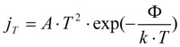
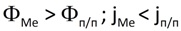
Let us create conditions where when a semiconductor, for example n-type, is in contact with a metal, the thermodynamic work function of the electrons from the metal would be greater than the thermodynamic work function of the electrons from the semiconductor. Under such conditions, according to Richardson's equation, the thermionic radiation current from the semiconductor surface will be greater than the thermionic radiation current from the metal surface:
At the initial moment of time, upon contact of these materials, the current from the semiconductor to the metal will exceed the reverse current (from the metal to the semiconductor), as a result of which in the near-surface regions of both semiconductors and metal, space charges will begin to accumulate — positive in the semiconductor and negative — in the metal. In the area of contact, an electric field formed by these charges will arise and a bending of the energy bands will take place.
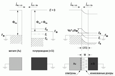
Under the action of the field, the thermodynamic work function for the semiconductor will increase and the increase will continue until the thermodynamic work functions and the corresponding thermionic radiation currents applied to the surface become equal in the contact region.
The picture of the transition to an equilibrium state with the formation of a potential barrier for p-type semiconductor and metal is similar to the considered example with n-type semiconductor and metal. The role of the external voltage is to regulate the height of the potential barrier and the strength of the electric field in the space charge region of the semiconductor.
The figure above shows the area diagrams of the various stages of Schottky barrier formation. Under equilibrium conditions in the contact zone, the thermal emission currents equalize, due to the effect of the field, a potential barrier appears, the height of which is equal to the difference between the thermodynamic work functions: φk = FMe — Фп / п.
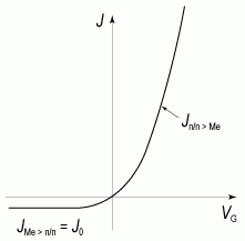
Obviously, the current-voltage characteristic for the Schottky barrier turns out to be asymmetric. In the forward direction, the current increases exponentially with the applied voltage. In the opposite direction, the current does not depend on the voltage. In both cases, the current is driven by electrons as the main charge carriers.
Therefore, Schottky diodes are distinguished by their speed, since they exclude diffuse and recombination processes that require additional time. The dependence of the current on the voltage is related to a change in the number of carriers, since these carriers are involved in the charge transfer process. The external voltage changes the number of electrons that can pass from one side of the Schottky barrier to the other side.
Due to the manufacturing technology and based on the described principle of operation, Schottky diodes have a low voltage drop in the forward direction, much smaller than that of traditional p-n-diodes.
Here, even a small initial current through the contact area leads to the release of heat, which then contributes to the appearance of additional current carriers. In this case, there is no injection of minority charge carriers.
Schottky diodes therefore have no diffuse capacitance as there are no minority carriers and as a result the speed is quite high compared to semiconductor diodes. It turns out to be a semblance of a sharp asymmetric p-n junction.
Thus, first of all, Schottky diodes are microwave diodes for various purposes: detector, mixing, avalanche transit, parametric, pulsed, multiplying. Schottky diodes can be used as radiation detectors, strain gauges, nuclear radiation detectors, light modulators and finally high frequency rectifiers.

Schottky diode designation on diagrams
Diode Schottky today
Today, Schottky diodes are widely used in electronic devices. In the diagrams, they are depicted differently from conventional diodes. You can often find dual Schottky rectifiers made in the three-pin housing typical of power switches. Such dual structures contain two Schottky diodes inside, joined by cathodes or anodes, more often than cathodes.
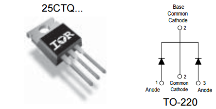
The diodes in the assembly have very similar parameters, since each such node is produced in one technological cycle, and as a result, their operating temperature is accordingly the same and the reliability is higher. A sustained voltage drop of 0.2-0.4 volts along with high speed (units of nanoseconds) are the undoubted advantages of Schottky diodes over their p-n counterparts.
The peculiarity of the Schottky barrier in diodes, in connection with a low voltage drop, is manifested at applied voltages of up to 60 volts, although the speed remains steadfast. Today, Schottky diodes of the 25CTQ045 type (for voltages up to 45 volts, for currents up to 30 amperes for each pair of diodes in the assembly) can be found in many switching power supplies, where they serve as rectifiers for currents up to several hundred kilohertz.
It is impossible not to touch on the topic of the disadvantages of Schottky diodes, of course they are and there are two of them. First, a short-term excess of the critical voltage will immediately disable the diode. Second, temperature strongly affects the maximum reverse current. At a very high junction temperature, the diode will simply break even when operating at rated voltage.
No radio amateur can do without Schottky diodes in his practice. The most popular diodes can be noted here: 1N5817, 1N5818, 1N5819, 1N5822, SK12, SK13, SK14. These diodes are available in both output and SMD versions. The main thing that radio amateurs appreciate them so much is their high speed and low junction voltage drop — a maximum of 0.55 volts — at a low cost of these components.
A rare PCB does without Schottky diodes for one purpose or another. Somewhere the Schottky diode serves as a low-power rectifier for the feedback circuit, somewhere - as a voltage stabilizer at the level of 0.3 - 0.4 volts, and somewhere it is a detector.
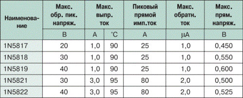
In the table below you can see the parameters of the most common low-power Schottky diodes today.