Transistor Electronic Switch - Principle of Operation and Schematic
 In pulse devices you can often find transistor switches. Transistor switches are found in flip-flops, switches, multivibrators, blocking generators, and other electronic circuits. In each circuit, the transistor switch performs its function, and depending on the operation mode of the transistor, the circuit of the switch as a whole may change, but the basic schematic diagram of the transistor switch is as follows:
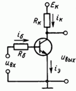
There are several basic modes of operation of a transistor switch: normal active mode, saturation mode, cut-off mode, and active reverse mode. Although the transistor switch circuit is basically a common emitter transistor amplifier circuit, this circuit differs in function and mode from a typical amplifier.
In a key application, the transistor serves as a fast switch, and the main static states are two: the transistor is off and the transistor is on. Latched State — Opened state when the transistor is in cutoff mode.Closed state - the saturation state of the transistor or a state close to saturation, in which state the transistor is open. When the transistor switches from one state to another, it is an active mode in which the processes in the cascade are non-linear.
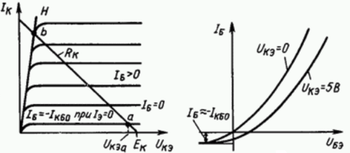
Static states are described according to the static characteristics of the transistor. There are two characteristics: the output family — the dependence of the collector current on the collector-emitter voltage and the input family — the dependence of the base current on the base-emitter voltage.
The cutoff mode is characterized by the biasing of the two pn junctions of the transistor in the opposite direction, and there is a deep cutoff and a shallow cutoff. A deep breakdown is when the voltage applied to the junctions is 3-5 times higher than the threshold and has the opposite polarity to the operating one. In this state, the transistor is open, and the currents at its electrodes are extremely small.
In a shallow break, the voltage applied to one of the electrodes is lower and the electrode currents are higher than in a deep break, with the result that the currents are already dependent on the applied voltage according to the lower curve of the output characteristic family , this curve is called the «limiting characteristic» ...
For example, we will perform a simplified calculation for the key mode of the transistor that will operate on a resistive load. A transistor will remain for a long time in only one of two basic states: fully open (saturation) or fully closed (cutoff).
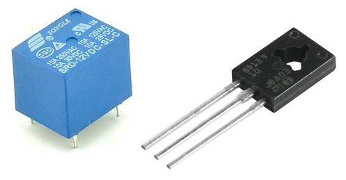
Let the transistor load be the coil of the relay SRD-12VDC-SL-C, whose coil resistance at nominal 12 V will be 400 ohms.We ignore the inductive nature of the relay coil, let the developers provide a silencer to protect against transient emissions, but we will calculate based on the fact that the relays will turn on once and for a very long time. We find the collector current by the formula:
Ik = (Upit-Ukenas) / Rn.
Where: Ik — direct current of the collector; Usup — supply voltage (12 volts); Ukenas — saturation voltage of the bipolar transistor (0.5 volts); Rn — load resistance (400 Ohm).
We get Ik = (12-0.5) / 400 = 0.02875 A = 28.7 mA.
For fidelity, let's take a transistor with a margin for the limiting current and the limiting voltage. A BD139 in a SOT-32 package will do. This transistor has parameters Ikmax = 1.5 A, Ukemax = 80 V. There will be a good margin.
In order to provide a collector current of 28.7 mA, a suitable base current must be provided. The base current is determined by the formula: Ib = Ik / h21e, where h21e is the static current transfer coefficient.
Modern multimeters allow you to measure this parameter, and in our case it was 50. So Ib = 0.0287 / 50 = 574 μA. If the value of the coefficient h21e is unknown, for reliability you can take the minimum from the documentation for this transistor.
To determine the required base resistor value. The saturation voltage of the main emitter is 1 volt. This means that if the control is carried out by a signal from the output of a logic microcircuit, the voltage of which is 5 V, then to provide the necessary base current of 574 μA, with a drop at a 1 V transition, we get:
R1 = (Uin-Ubenas) / Ib = (5-1) / 0.000574 = 6968 Ohm
Let's choose the smaller side (so that the current is fully sufficient) of the standard series 6.8 kOhm resistor.
BUT, in order for the transistor to switch faster and the operation is reliable, we will use an additional resistor R2 between the base and the emitter, and some power will fall on it, which means that it is necessary to reduce the resistance of the resistor R1. Let's take R2 = 6.8 kΩ and adjust the value of R1:
R1 = (Uin-Ubenas) / (Ib + I (via resistor R2) = (Uin-Ubenas) / (Ib + Ubenas / R2)
R1 = (5-1) / (0.000574 + 1/6800) = 5547 ohms.
Let R1 = 5.1 kΩ and R2 = 6.8 kΩ.
Let's calculate the switch losses: P = Ik * Ukenas = 0.0287 * 0.5 = 0.014 W. The transistor does not need a heatsink.