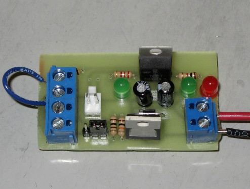
Transistor switching circuits with field effects
Just as in various electronic devices bipolar transistors operate with common emitter, common collector or common base switching, field effect transistors in many cases it can be used similarly to include: common source, common drain, or common gate.
The difference lies in the control method: the bipolar transistor is controlled by the base current and the FET is controlled by the gate charge.
In terms of control power consumption, FET control is generally more economical than bipolar transistor control. This is one of the factors that explain the current popularity of field-effect transistors. However, consider in general terms the typical switching circuits of FETs.
General source switching
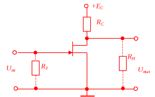
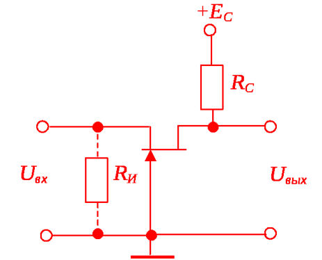
The circuit for turning on a common-source FET is analogous to a common-emitter circuit for a bipolar transistor. Such inclusion is very common due to the ability to give a significant increase in power and current while the voltage phase of the drain circuit is reversed.
The input resistance of the direct junction-source reaches hundreds of megohms, although it can be reduced by adding a resistor between the gate and the source to galvanically pull the gate to the common wire (protecting the FET from pickups).
The value of this resistor Rz (typically 1 to 3 MΩ) is chosen so as not to greatly bias the gate-source resistance, while preventing overvoltage from the reverse bias control node current.
The significant input resistance of an FET in a common-source circuit is an important advantage of the FET when used in voltage, current and power amplification circuits, since the resistance in the drain circuit Rc usually does not exceed a few kΩ.
Turn on with common source
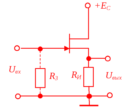
The switching circuit of a common-drain (source-follower) FET is analogous to a common-collector circuit for a bipolar transistor (emitter-follower). Such switching is used in matching stages where the output voltage must be in phase with the input voltage.
The input resistance of the gate-source junction, as before, reaches hundreds of megohms, while the output resistance Ri is relatively small. This switching has a higher frequency range than a simple source circuit. The voltage gain is close to unity because the source-drain and gate-source voltages for this circuit are usually close in magnitude.
General shutter switching
A common gate circuit is similar to a common base stage for a bipolar transistor. There is no current gain here, and therefore the power gain is many times less than in a common-source cascade.The boost voltage has the same phase as the control voltage.
Since the output current is equal to the input current, then the current gain is equal to unity and the voltage gain is usually greater than unity.
This switching has a characteristic - parallel negative current feedback, since with an increase in the control input voltage, the source potential increases, correspondingly, the drain current decreases and the voltage across the source circuit resistance Ri decreases.
So, on the one hand, the voltage across the source resistance increases due to increasing input signal, but decreases as the drain current decreases, this is negative feedback.
This phenomenon widens the stage bandwidth in the high-frequency region, which is why the common gate circuit is popular in high-frequency voltage amplifiers and is particularly sought after in highly stable resonant circuits.