PFC controller L6561
In one of the previous articles, we considered the general principle of operation. active power correctors (KKM or PFC). However, no correction circuit will work without a controller, whose task is to correctly organize the control of the field-effect transistor in the general circuit.
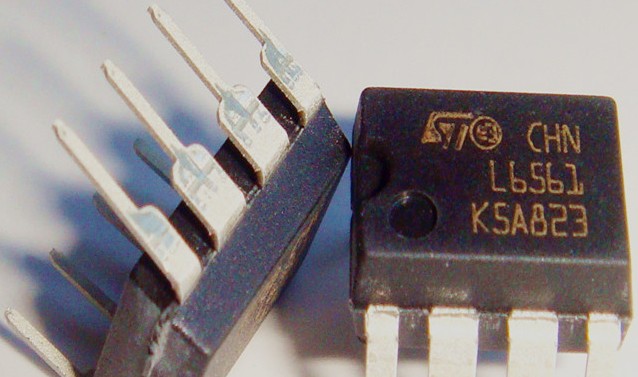
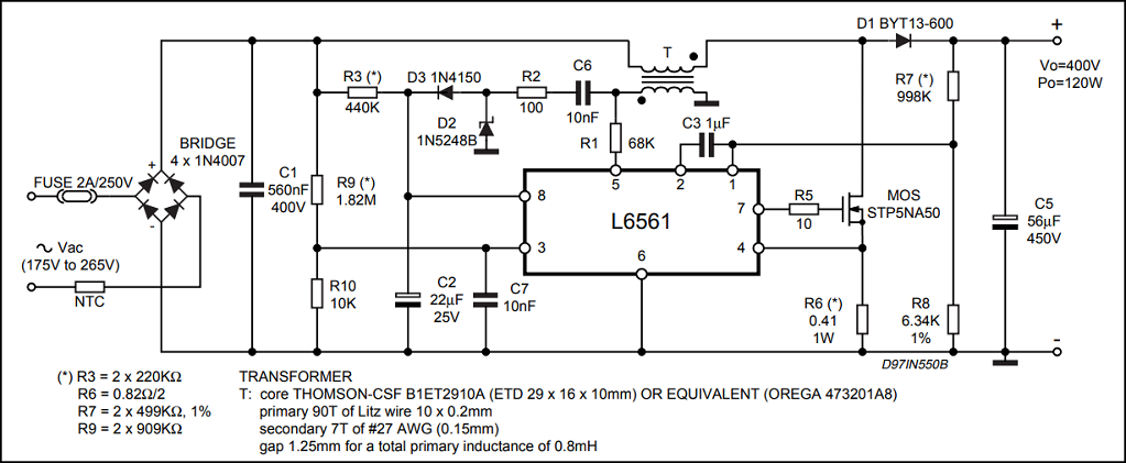
As a vivid example of a universal PFC controller for PFC implementation, the popular L6561 microcircuit can be cited, which is available in SO-8 and DIP-8 packages and is designed to build power factor correction blocks of the network with a nominal value of up to 400 W (without using an additional external port driver).
The Boost-PWM control mode, which is specific to this controller, achieves a power factor of up to 0.99 with current distortion within 5% at a primary AC voltage of 85 to 265 volts. Next, we will look at the purpose of the pins of the microcircuit and a typical circuit for its use.
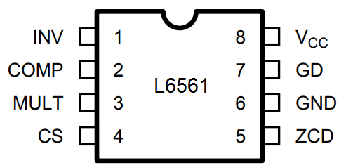
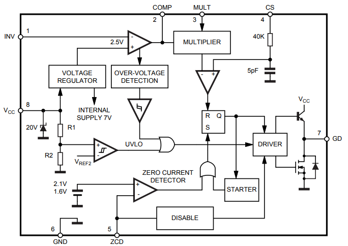
This output is the inverting input of the error amplifier, whose task is to measure in real time the DC voltage of the output capacitor of the converter in order to keep it constant and without exceeding it.The output voltage is measured with a resistive divider.
The threshold voltage of the amplifier here is 2.5 volts. It does not matter what output voltage the converter is designed for: 240, 350, 400 volts, — if the voltage on the lower arm of the resistive divider reaches the threshold of 2.5 volts, at that moment the operation of the internal driver of the output stage is blocked and is prevented by - further increasing the output voltage. An input current in the range of 250-400 μA is sufficient to operate the error amplifier.
Conclusion # 2 — COMP — compensation network
This pin is the output of the comparator of the error amplifier, it is designed to adjust the frequency response correction circuit of the external amplifier. The purpose for which external components are added here is to protect against parasitic self-excitation of the closed-loop voltage feedback amplifier. We won't go into theory, just note this aspect.
Conclusion # 3 — MULT — Multiplier
To this output, through a resistive divider, which is installed at the input immediately after the rectifier and the film capacitor, a rectified alternating voltage is supplied, the shape of which is sinusoidal, and its amplitude reaches 3.5 volts, and each time this voltage is proportional to the amplitude of the rectified voltage supplied to the operating choke.
Thus, through this input, the controller receives information about the current phase of the sinusoid (more precisely, its half, obtained by rectifying the diode bridge) of the voltage supplied to the converter — this is the reference sinusoidal signal for the current loop.
Conclusion # 4 — CS — current sensor
This input is supplied with voltage from the current shunt which is installed in the source circuit of the FET.The threshold voltage is here from 1.6 to 1.8 volts, from this moment the current within the period no longer increases, since this threshold is considered the limit for the field-effect transistor. This pin serves to protect the FET from overcurrent by adjusting the operating pulse width (PWM), — as soon as the current limit is reached, the control pulse of the current transistor immediately stops and the driver releases the gate.
Conclusion # 5 — ZCD — Zero Current Detector
This pin is supplied with voltage from the zero current sensor, which comes from an additional inductor coil connected to the chip through a resistor. When the next cycle of energy transfer from the choke to the load is completed, the current in the choke drops to zero, therefore the voltage of the additional coil will be zero. At this point, the zero detector comparator gives the command to start the next unlock cycle of the external transistor to work out the next choke energy accumulation period, and so on. in Circle.
PIN # 6 — GND — Ground
A common wire, ground bus, is connected here.
Conclusion number 7 — GD — Gate driver output
Push-pull driver for external control of the transistor. This output stage is capable of delivering a peak drive current of 400mA (gate charge and discharge). If this amount of current is small, then you can resort to connecting an external, more powerful port driver.
Conclusion #8 — Vcc — Supply voltage
The positive input power referenced to GND is rated for 11 to 18 volts. It is possible to power it directly from the auxiliary inductor coil (from the zero current sensor coil) as suggested in the data sheet of the chip.When supplied with a voltage of 12 volts, when the switch operates at a frequency of 70 kHz and with a gate capacitance of 1 nF, the microcircuit consumes a current of up to 5.5 mA. The datasheet provides a diagram for obtaining a stabilized voltage to power the chip using zener diode 1N5248B.