What is an electron hole p-n junction
Semiconductors include substances with a resistance of 10-5 to 102 ohm x m. In terms of their electrical properties, they occupy an intermediate position between metals and insulators.
The resistance of a semiconductor is affected by many factors: it strongly depends on the temperature (the resistance decreases with increasing temperature), it depends on the lighting (the resistance decreases under the influence of light), etc.
Depending on the type of impurities in the semiconductor, one of the conductivities prevails — electron (n-type) or hole (p-type).
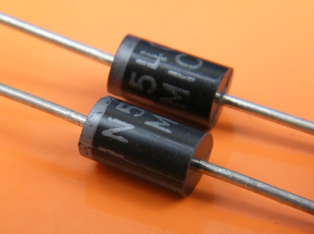
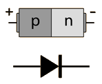
The main part of any semiconductor device (diode, LED, transistor, thyristor, etc.) is the so-called. P-electron hole-junction. It is obtained if part of the crystal has n-type conductivity and the other part has p-type conductivity. Both regions must be obtained in one monolithic crystal with the same lattice. A p-n-junction cannot be obtained by mechanically connecting two crystals with different types of conductivity.
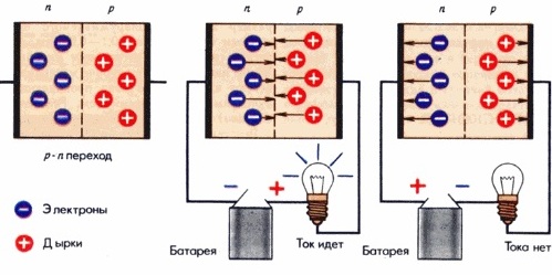
The main current carriers are holes in the p-region and free electrons in n-regions — diffused from one region to another.Due to the recombination (mutual neutralization of charges) of electrons and holes between p and n, a semiconductor layer depleted of current carriers (blocking layer) is formed.
The excess charge is created by negative ions of the p-region and positive ions of the n-region, and the entire volume of the semiconductor as a whole remains electrically neutral. As a result, at the p-n junction, an electric field directed from the n-plane to the p-region arises and prevents further diffusion of holes and electrons.
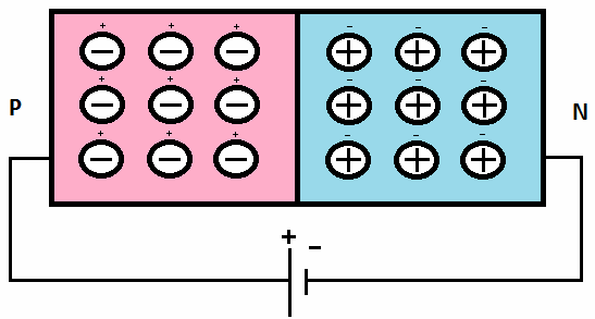
In the p-n-transition, an electric potential difference is formed, that is, a so-called potential barrier arises. The potential distribution in the transition layer depends on the distance. Potential zero is usually taken to be the potential in the p-region directly near a p-n-junction where there is no space charge.
It can be shown that the p-n junction has a rectifying property. If the negative pole of a DC voltage source is connected to the p-region, then the potential barrier will increase with the value of the applied voltage and the main current carriers will not be able to pass through the p-n junction. Then semiconductor rectifier there will be a very high resistance and the so-called reverse current will be very small.
However, if we attach a positive to the p-region, and to the n-region Cc the negative pole of the source, then the potential barrier will decrease and the main current carriers will be able to pass through the p-n junction. In the chain will appear the so-called A forward current that will increase as the source voltage increases.
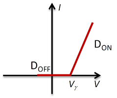
Current-voltage characteristic of the diode
So an electron path-hole — a junction between two regions of semiconductors, one of which has n-type electrical conductivity and the other is p-type. The electron-hole junction serves as the basis for semiconductor devices. In the transition region, a space charge layer is formed, depleted in mobile charge carriers. This layer represents a potential barrier for the majority and a potential well for minority charge carriers. The main property of the electron-hole transition is unipolar conduction.
Nonlinear semiconductor elements with unbalanced current-voltage characteristics are widely used to convert AC to DC... Such elements with unidirectional conductivity are called rectifiers or electric valves.