The device and principle of operation of the transistor
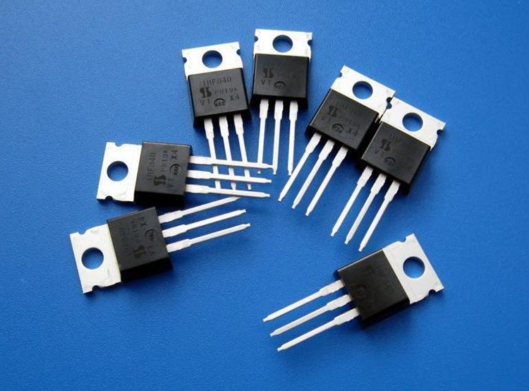
The practical importance of the bipolar transistor to modern electronics and electrical engineering cannot be overstated. Bipolar transistors are used everywhere today: to generate and amplify signals, in electrical converters, in receivers and transmitters and in many other places, it can be listed for a very long time.
Therefore, within the framework of this article, we will not touch on all possible areas of application of bipolar transistors, but only consider the device and the general principle of operation of this wonderful semiconductor device, which from the 1950s turned the entire electronics industry and since the 1970s contributed significantly to the acceleration of technical progress.
A bipolar transistor is a three-electrode semiconductor device that includes three bases of variable conductivity as the base. Thus, transistors are of the NPN and PNP types. Semiconductor materials from which transistors are made are mainly: silicon, germanium, gallium arsenide and others.
Silicon, germanium, and other substances are initially dielectrics, but if you add impurities to them, they become semiconductors. Additions to silicon such as phosphorus (an electron donor) will make silicon an N-type semiconductor, and if boron (an electron acceptor) is added to silicon, then the silicon will become a P-type semiconductor.
As a result, N-type semiconductors have electron conduction and P-type semiconductors have hole conduction. As you understand, conductivity is determined by the type of operating charge carriers.
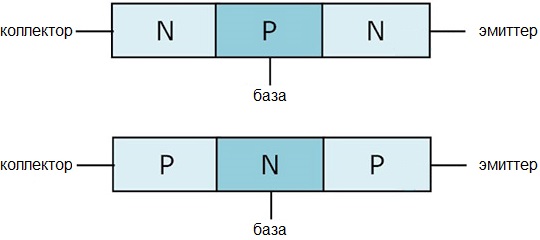
So, a three-layer pie of P-type and N-type semiconductors is essentially a bipolar transistor. Attached to each layer are terminals called: Emitter, Collector and Base.
The base is a conductivity control electrode. The emitter is the source of current carriers in the circuit. The collector is the place in the direction of which the current carriers rush under the action of the EMF applied to the device.
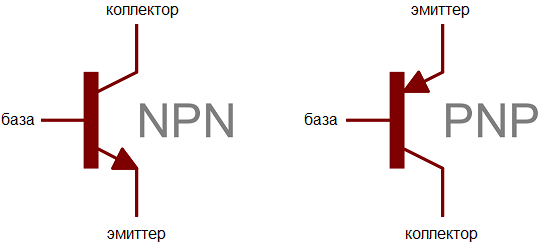
The symbols for NPN and PNP bipolar transistors are different in the diagrams. These designations only reflect the device and the principle of operation of the transistor in the electrical circuit. The arrow is always drawn between the emitter and the base. The direction of the arrow is the direction of the control current that is fed into the base emitter circuit.
So, in an NPN transistor, the arrow points from the base to the emitter, which means that in active mode, electrons from the emitter will rush to the collector, while the control current must be directed from the base to the emitter.
In a PNP transistor, it is just the opposite: the arrow is directed from the emitter to the base, which means that in active mode the holes from the emitter rush to the collector, while the control current must be directed from the emitter to the base.
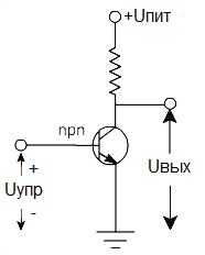
Let's see why this happens. When a constant positive voltage is applied to the base of an NPN transistor (in the region of 0.7 volts) relative to its emitter, the base-emitter pn junction of this NPN transistor (see figure) is forward biased, and the potential barrier between the collector junction -base and the base emitter decreases, now electrons can move through it under the action of the EMF in the collector-emitter circuit.
With sufficient base current, a collector-emitter current will arise in this circuit and collect with the base-emitter current. The NPN transistor will turn on.
The relationship between the collector current and the control current (base) is called the current gain of the transistor. This parameter is given in the transistor documentation and can vary from units to several hundreds.
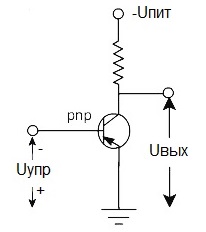
When a constant negative voltage is applied to the base of a PNP transistor (in the region of -0.7 volts) relative to its emitter, the np base-emitter junction of this PNP transistor is forward biased, and the potential barrier between the collector-base and base junction -emitter decreases, now holes can move through it under the action of the EMF in the collector-emitter circuit.
Note the polarity of the supply to the collector circuit. With sufficient base current, a collector-emitter current will arise in this circuit and collect with the base-emitter current. The PNP transistor will turn on.
Bipolar transistors are commonly used in various devices in amplifier, barrier or switch.
In boost mode, the base current never falls below the holding current, which keeps the transistor in an open conducting state at all times. In this mode, low base current oscillations initiate corresponding oscillations at a much higher collector current.
In the key mode, the transistor switches from a closed to an open state, acting as a high-speed electronic switch. In barrier mode, by changing the base current, the load current included in the collector circuit is controlled.
See also:Transistor Electronic Switch - Principle of Operation and Schematic