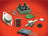
Semiconductor Devices - Types, Overview and Uses
 The rapid development and expansion of the fields of application of electronic devices is due to the improvement of the element base on which semiconductor devices are based... Therefore, in order to understand the processes of functioning of electronic devices, it is necessary to know the device and the principle of operation of the main types of semiconductor devices.
Semiconductor materials in terms of their specific resistance, they occupy an intermediate position between conductors and dielectrics.
The main materials for the manufacture of semiconductor devices are silicon (Si), silicon carbide (SiC), gallium and indium compounds.
Semiconductor conductivity depends on the presence of impurities and external energy influences (temperature, radiation, pressure, etc.). Current flow is caused by two types of charge carriers — electrons and holes. Depending on the chemical composition, a distinction is made between pure and impurity semiconductors.
For the production of electronic devices, solid semiconductors with a crystalline structure are used.
Semiconductor devices are devices whose operation is based on the use of the properties of semiconductor materials.
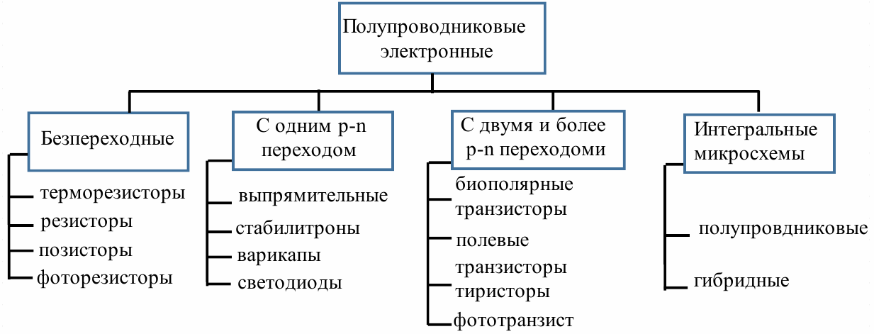
Classification of semiconductor devices
Based on continuous semiconductors, semiconductor resistors:
Linear Resistor - Resistance depends slightly on voltage and current. It is an "element" of integrated circuits.
Varistor - the resistance depends on the applied voltage.
Thermistor - resistance depends on temperature. There are two types: thermistor (as the temperature increases, the resistance decreases) and posistors (as the temperature increases, the resistance increases).
Photoresistor — the resistance depends on the illumination (radiation). Deformer — resistance depends on mechanical deformation.
The principle of operation of most semiconductor devices is based on the electron-hole junction p-n-junction properties.
Semiconductor diodes
It is a semiconductor device with one p-n junction and two terminals, the operation of which is based on the properties of the p-n junction.
The main property of the p-n junction is unidirectional conduction - the current flows in only one direction. The conventional graphic designation (UGO) of the diode has the form of an arrow, which indicates the direction of current flow through the device.
Structurally, the diode consists of a p-n junction enclosed in a case (with the exception of micromodule open frames) and two terminals: from the p-region-anode, from the n-region-cathode.
These. A diode is a semiconductor device that conducts current in only one direction—from the anode to the cathode.
The dependence of the current through the device on the applied voltage is called the current-voltage characteristic (VAC) device I = f (U).The single-sided conduction of the diode is evident from its I-V characteristic (Fig. 1).
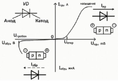
Figure 1 — Diode current-voltage characteristic
Depending on the purpose, semiconductor diodes are divided into rectifier, universal, pulse, zener diodes and stabilizers, tunnel and reverse diodes, LEDs and photodiodes.
The one-sided conduction determines the rectification properties of the diode. With direct connection («+» to the anode and «-» to the cathode) the diode is open and a sufficiently large forward current flows through it. In reverse («-» to the anode and «+» to the cathode), the diode is closed, but a small reverse current flows.
Rectifier diodes are designed to convert low-frequency alternating current (usually less than 50 kHz) into direct current, i.e. to stand up. Their main parameters are the maximum allowable forward current Ipr max and the maximum allowable reverse voltage Uo6p max. These parameters are called limiting — exceeding them can partially or completely disable the device.
To increase these parameters, diode columns, nodes, matrices are made, which are series-parallel, bridge or other connections of p-n-junctions.
Universal diodes are used to rectify currents in a wide frequency range (up to several hundred megahertz). The parameters of these diodes are the same as those of the rectifier diodes, only additional ones are entered: the maximum operating frequency (MHz) and the diode capacitance (pF).
Pulse diodes are designed for pulse signal conversion, they are used in high-speed pulse circuits.The requirements for these diodes are related to ensuring a fast response of the device to the impulse nature of the supplied voltage — a short transition time of the diode from the closed state to the open state and vice versa.
Zener diodes — these are semiconductor diodes, the voltage drop across which depends little on the current flowing. It serves to stabilize the voltage.
Varikapi - the principle of operation is based on the property of the p-n-junction to change the value of the barrier capacitance when the value of the reverse voltage changes on it. They are used as voltage controlled variable capacitors. In the schemes, the varicaps are turned on in the opposite direction.
LEDs - these are semiconductor diodes, the principle of which is based on the emission of light from a p-n junction when a direct current passes through it.
Photodiodes - the reverse current depends on the illumination of the p-n-junction.
Schottky diodes - based on a metal-semiconductor junction, which is why they have a significantly higher response rate than conventional diodes.
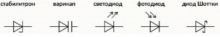
Figure 2 — Conventional graphical representation of diodes
For more information on diodes see here:
Parameters and schemes of the rectifier
Photodiodes: device, characteristics and principles of operation
Transistors
A transistor is a semiconductor device designed to amplify, generate, and convert electrical signals, as well as switch electrical circuits.
A distinctive feature of the transistor is the ability to amplify voltage and current — voltages and currents acting at the input of the transistor lead to the appearance of significantly higher voltages and currents at its output.
With the spread of digital electronics and pulse circuits, the main property of the transistor is its ability to be in the open and closed state under the influence of a control signal.
The transistor got its name from the abbreviation of two English words tran (sfer) (re) sistor - controlled resistor. This name is not accidental, because under the action of the input voltage applied to the transistor, the resistance between its output terminals can be adjusted in a very wide range.
The transistor allows you to adjust the current in the circuit from zero to the maximum value.
Classification of transistors:
— according to the principle of action: field (unipolar), bipolar, combined.
— by the value of the dissipated power: low, medium and high.
— by the value of the limiting frequency: low, medium, high and ultra-high frequency.
— by the value of the operating voltage: low and high voltage.
— by functional purpose: universal, reinforcing, key, etc.
-in terms of design: with an open frame and in a box-type version, with rigid and flexible terminals.
Depending on the functions performed, transistors can work in three modes:
1) Active mode - used to amplify electrical signals in analog devices. The resistance of the transistor changes from zero to the maximum value - they say that the transistor "opens" or "closes".
2) Saturation mode — the resistance of the transistor tends to zero. In this case, the transistor is equivalent to a closed relay contact.
3) Cut-off mode — the transistor is closed and has a high resistance, i.e. it is equivalent to an open relay contact.
The saturation and cutoff modes are used in digital, pulse, and switching circuits.
A bipolar transistor is a semiconductor device with two p-n junctions and three conductors providing power amplification of electrical signals.
In bipolar transistors, the current is caused by the movement of charge carriers of two types: electrons and holes, which accounts for their name.
On the diagrams, it is allowed to depict transistors, both in a circle and without it (Fig. 3). The arrow shows the direction of current flow in the transistor.
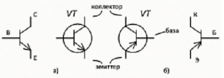
Figure 3-Conventional-graphic notation of transistors n-p-n (a) and p-n-p (b)
The basis of the transistor is a semiconductor plate, in which three sections with a variable type of conductivity - electron and hole - are formed. Depending on the alternation of the layers, two types of transistor structure are distinguished: n-p-n (Fig. 3, a) and p-n-p (Fig. 3, b).
Emitter (E) — a layer that is a source of charge carriers (electrons or holes) and creates a current on the device;
Collector (K) — a layer that accepts charge carriers coming from the emitter;
Base (B) — the middle layer that controls the current of the transistor.
When the transistor is connected to the circuit, one of its electrodes is input (the source of the input alternating signal is on), the other is output (the load is on), the third electrode is common to the input and output. In most cases, a common emitter circuit is used (Figure 4). A voltage of no more than 1 V is applied to the base, more than 1 V to the collector, for example +5 V, +12 V, +24 V, etc.
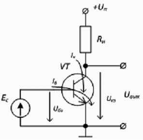
Figure 4 — Circuit diagrams of a common emitter bipolar transistor
The collector current occurs only when the base current Ib (determined by Ube) is flowing.The more Ib, the more Ik. Ib is measured in units of mA, and the collector current is measured in tens and hundreds of mA, i.e. IbIk. Therefore, when a small amplitude AC signal is applied to the base, the small Ib will change and the large Ic will change in proportion to it. When a load resistance collector is included in the circuit, a signal will be distributed to it, repeating the shape of the input, but with a larger amplitude, i.e. amplified signal.
The maximum permissible parameters of the transistors include, first of all: the maximum permissible power dissipated on the collector Pk.max, the voltage between the collector and the emitter Uke.max, the collector current Ik.max.
To increase the limiting parameters, transistor assemblies are produced, which can number up to several hundred parallel-connected transistors enclosed in a single housing.
Bipolar transistors are now used less and less, especially in pulsed power technology. They are replaced by MOSFETs and combined IGBTs, having indisputable advantages in this field of electronics.
In field-effect transistors, the current is determined by the movement of carriers of only one sign (electrons or holes). Unlike bipolar, transistor current is driven by an electric field that changes the cross-section of the conducting channel.
Since there is no input current in the input circuit, the power consumption of this circuit is practically zero, which is undoubtedly an advantage of the field-effect transistor.
Structurally, a transistor consists of an n- or p-type conducting channel, at the ends of which there are regions: a source that emits charge carriers and a drain that accepts carriers.The electrode used to adjust the cross-section of the channel is called the gate.
A field-effect transistor is a semiconductor device that regulates the current in a circuit by changing the cross-section of the conducting channel.
There are field-effect transistors with a gate in the form of a pn junction and with an isolated gate.
In field-effect transistors with an insulated gate between the semiconductor channel and the metal gate there is an insulating layer of dielectric - MIS transistors (metal - dielectric - semiconductor), a special case - silicon oxide - MOS transistors.
A built-in channel MOS transistor has an initial conductance that, in the absence of an input signal (Uzi = 0), is approximately half of the maximum. In MOS transistors with an induced channel at a voltage Uzi = 0, the output current is absent, Ic = 0, because initially there is no conducting channel.
MOSFETs with an induced channel are also called MOSFETs. They are mainly used as key elements, for example in switching power supplies.
The key elements based on MOS transistors have a number of advantages: the signal circuit is not galvanically connected to the source of the control action, the control circuit does not consume current and has double-sided conductivity. Field-effect transistors, unlike bipolar ones, are not afraid of overheating.
For more information on transistors see here:
Thyristors
A thyristor is a semiconductor device operating in two steady states — low conduction (thyristor closed) and high conduction (thyristor open). Structurally, a thyristor has three or more p-n junctions and three outputs.
In addition to the anode and cathode, a third output (electrode) is provided in the design of the thyristor, which is called the control.
The thyristor is designed for non-contact switching (on and off) of electrical circuits. They are characterized by high speed and the ability to switch currents of a very significant magnitude (up to 1000 A). They are gradually being replaced by switching transistors.
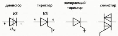
Figure 5 - Conventional - graphical designation of thyristors
Dynistors (two-electrode) — like conventional rectifiers, they have an anode and a cathode. As the forward voltage increases at a certain value Ua = Uon, the dinistor opens.
Thyristors (SCRs — three-electrode) — have an additional control electrode; Uin is changed by the control current flowing through the control electrode.
To transfer the thyristor to the closed state, it is necessary to apply a reverse voltage (- to the anode, + to the cathode) or reduce the forward current below a value called the Iuder holding current.
Locking thyristor - can be switched to the closed state by applying a control pulse of reverse polarity.
Thyristors: principle of operation, design, types and methods of inclusion
Triacs (symmetric thyristors) — conducting current in both directions.
Thyristors are used as proximity switches and controllable rectifiers in automation devices and electrical current converters. In alternating and pulsed current circuits, it is possible to change the time of the open state of the thyristor, and hence the time of current flow through the load. This allows you to adjust the power distributed to the load.