Semiconductor conductivity
Substances capable of conducting or not conducting an electric current are not limited to a strict division of only conductors and dielectrics. There are also semiconductors, such as silicon, selenium, germanium, and other minerals and alloys worthy of being separated as a separate group.
These substances conduct electric current better than dielectrics, but worse than metals, and their conductivity increases with increasing temperature or illumination. This characteristic of semiconductors makes them applicable in light and temperature sensors, but their main application is still electronics.
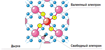
If you look, for example, at a silicon crystal, you can find that silicon has a valency of 4, that is, on the outer shell of its atom there are 4 electrons that are bonded to four neighboring silicon atoms in the crystal. If such a crystal is affected by heat or light, then the valence electrons will receive an increase in energy and leave their atoms, becoming free electrons - an electron gas will appear in the open volume of the semiconductor - as in metals, that is, it will a holding condition occurs.
But unlike metals, semiconductors differ in their conductivity of electrons and holes. Why is this happening and what is it? When the valence electrons leave their sites, regions of a lack of negative charge—“holes”—are formed in those former sites, which now have an excess of positive charge.
The neighboring electron will easily jump into the resulting «hole», and as soon as this hole is filled with the electron that jumped into it, a hole forms again in place of the jumped electron.
That is, it turns out that a hole is a positively charged moving region of a semiconductor. And when a semiconductor is connected to a circuit with an EMF source, the electrons will move to the positive terminal of the source and the holes to the negative terminal. This is how the internal conductivity of the semiconductor takes place.
The movement of holes and conduction electrons in a semiconductor without an applied electric field will be chaotic. If an external electric field is applied to the crystal, then the electrons inside it will move against the field, and the holes will move along the field, that is, the phenomenon of internal conduction will occur in the semiconductor, which will not only be caused by electrons, but also by holes .
In a semiconductor, conduction always occurs only under the influence of some external factors: due to irradiation with photons, from the effect of temperature, when electric fields are applied, etc.
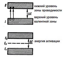
The Fermi level in a semiconductor falls in the middle of the band gap. The transition of the electron from the upper valence band to the lower conduction band requires an activation energy equal to the bandgap delta (see figure). And as soon as an electron appears in the conduction band, a hole is created in the valence band. Thus, the energy spent is divided equally during the formation of a pair of current carriers.
Half of the energy (corresponding to half of the band width) is spent on electron transfer and half on hole formation; as a result, the origin corresponds to the middle of the strip width. The Fermi energy in a semiconductor is the energy at which electrons and holes are excited. The position that the Fermi level is located for a semiconductor in the middle of the band gap can be confirmed by mathematical calculations, but we omit the mathematical calculations here.
Under the influence of external factors, for example, when the temperature increases, the thermal vibrations of the crystal lattice of a semiconductor lead to the destruction of some valence bonds, as a result of which some of the electrons become, separated, free charge carriers.
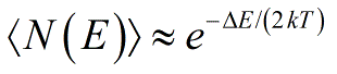
In semiconductors, along with the formation of holes and electrons, the recombination process takes place: electrons pass into the valence band from the conduction band, giving their energy to the crystal lattice and emitting quanta of electromagnetic radiation.Thus, each temperature corresponds to the equilibrium concentration of holes and electrons, which depends on the temperature according to the following expression:
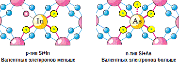
There is also impurity conductivity of semiconductors, when a slightly different substance is introduced into the crystal of a pure semiconductor that has a higher or lower valency than the parent substance.
If in pure, say, the same silicon, the number of holes and free electrons is equal, that is, they are formed all the time in pairs, then in the case of an impurity added to silicon, for example, arsenic, having a valence of 5, the number of holes will be less than the number of free electrons, that is, a semiconductor is formed with a large number of free electrons, negatively charged, it will be an n-type (negative) semiconductor. And if you mix indium, which has a valency of 3, which is less than that of silicon, then there will be more holes—it will be a p-type (positive) semiconductor.
Now, if we bring semiconductors of different conductivity into contact, then at the point of contact we get a p-n junction. Electrons moving from the n-region and holes moving from the p-region will begin to move towards each other, and on opposite sides of the contact there will be regions with opposite charges (on opposite sides of the pn-junction ) : a positive charge will accumulate in the n-region and a negative charge in the p-region. The different parts of the crystal with respect to the transition will be oppositely charged. This position is very important for everyone's work. semiconductor devices.
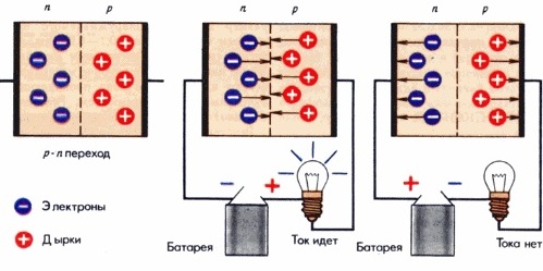
The simplest example of such a device is a semiconductor diode, where only one pn junction is used, which is enough to achieve the task — to conduct current in only one direction.
Electrons from the n-region move towards the positive pole of the power source and holes from the p-region move towards the negative pole. Sufficient positive and negative charges will accumulate near the junction, the resistance of the junction will decrease significantly and current will flow through the circuit.
In the reverse connection of the diode, the current will come out tens of thousands of times less, since the electrons and holes will simply be blown by an electric field in different directions from the junction. This principle works diode rectifier.