Bipolar transistors
 The term «bipolar transistor» is related to the fact that two types of charge carriers are used in these transistors: electrons and holes. For the manufacture of transistors, the same semiconductor materials are used as for diodes.
Bipolar transistors use a three-layer semiconductor structure made of semiconductors different electrical conductivity two p — n junctions are created with alternating types of electrical conductivity (p — n — p or n — p — n).
Bipolar transistors can be structurally unpackaged (Fig. 1, a) (for use, for example, as part of integrated circuits) and closed in a typical case (Fig. 1, b). The three pins of a bipolar transistor are called base, collector and emitter.
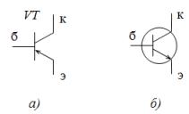
Rice. 1. Bipolar transistor: a) p-n-p-structures without a package, b) n-p-n-structures in a package
Depending on the general conclusion, you can get three connection schemes for a bipolar transistor: with a common base (OB), a common collector (OK) and a common emitter (OE). Let us consider the operation of a transistor in a common-base circuit (Fig. 2).
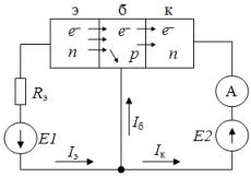
Rice. 2. Schematic of the bipolar transistor
The emitter injects (delivers) into the base the base carriers, in our n-type semiconductor device example, these will be electrons. The sources are chosen such that E2 >> E1. Resistor Re limits the current of the open p — n junction.
At E1 = 0, the current through the collector node is small (due to minority carriers), it is called the initial collector current Ik0. If E1> 0, the electrons overcome the p — n junction of the emitter (E1 turns on in the forward direction) and enter the core region.
The base is made with high resistance (low concentration of impurities), so the concentration of holes in the base is low. Therefore, the few electrons entering the base recombine with its holes, forming the base current Ib. At the same time, a much stronger field acts in the collector p — n junction on the E2 side than in the emitter junction, which attracts electrons to the collector. Therefore, most of the electrons reach the collector.
Emitter and collector currents are related emitter current transfer coefficient

at Ukb = const.
It is always ∆Ik < ∆Ie, and a = 0.9 — 0.999 for modern transistors.
In the considered scheme Ik = Ik0 + aIe »Ie. Therefore, the circuit Common base bipolar transistor has a low current ratio. Therefore, it is rarely used, mainly in high-frequency devices, where in terms of voltage gain it is preferable to others.
The basic switching circuit of a bipolar transistor is a common emitter circuit (Fig. 3).
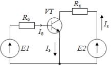
Rice. 3. Switching on a bipolar transistor according to the scheme with a common emitter
For her on Kirchhoff's first law we can write Ib = Ie — Ik = (1 — a) Ie — Ik0.
Given that 1 — a = 0.001 — 0.1, we have Ib << Ie » Ik.
Find the ratio of the collector current to the base current:
This relationship is called the base current transfer coefficient... At a = 0.99, we get b = 100. If a signal source is included in the base circuit, then the same signal, but amplified by the current b times, will flow in the collector circuit, forming voltage across the resistor Rk much greater than the signal source voltage...
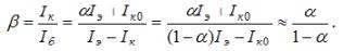
To evaluate the operation of a bipolar transistor over a wide range of pulsed and DC currents, powers and voltages, and to calculate the bias circuit, stabilize mode, families of input and output volt-ampere characteristics (VAC).
A family of input I — V characteristics establish the dependence of the input current (base or emitter) on the input voltage Ube at Uk = const, fig. 4, a. The input I — V characteristics of the transistor are similar to the I — V characteristics of a diode in direct connection.
The family of output I — V characteristics establishes the dependence of the collector current on the voltage across it at a certain base or emitter current (depending on the circuit with a common emitter or common base), fig. 4, b.
Rice. 4. Current-voltage characteristics of the bipolar transistor: a — input, b — output
In addition to the electrical n-p junction, a Schottky metal-semiconductor-barrier junction is widely used in high-speed circuits. In such transitions, no time is allocated for the accumulation and resorption of charges in the base, and the operation of the transistor depends only on the rate of recharge of the barrier capacitance.
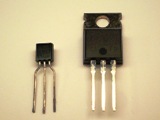
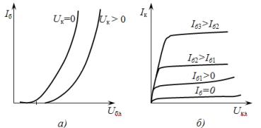
Rice. 5. Bipolar transistors
Parameters of bipolar transistors
The main parameters are used to evaluate the maximum permissible operating modes of the transistors:
1) maximum permissible collector-emitter voltage (for different transistors Uke max = 10 — 2000 V),
2) maximum permissible collector power dissipation Pk max — according to him, transistors are divided into low-power (up to 0.3 W), medium-power (0.3 — 1.5 W) and high-power (more than 1, 5 W), medium and high power transistors are often equipped with a special heatsink — a heatsink,
3) maximum permissible collector current Ik max — up to 100 A and more,
4) limiting current transmission frequency fgr (the frequency at which h21 becomes equal to unity), bipolar transistors are divided according to it:
- for low frequency — up to 3 MHz,
- medium frequency — from 3 to 30 MHz,
- high frequency — from 30 to 300 MHz,
- ultra-high frequency — more than 300 MHz.
Doctor of technical sciences, professor L.A. Potapov