IGBT transistors
 Bipolar transistors with an isolated gate are a new type of active devices that appeared relatively recently. Its input characteristics are similar to the input characteristics of a field effect transistor and its output characteristics are similar to the output characteristics of a bipolar.
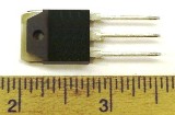
In the literature, this device is called an IGBT (Insulated Gate Bipolar Transistor)... In terms of speed, it is significantly superior bipolar transistors... Most often, IGBT transistors are used as power switches, where the turn-on time is 0.2 — 0.4 μs, and the turn-off time is 0.2 — 1.5 μs, the switched voltages reach 3.5 kV, and currents are 1200 A.
 IGBT-T transistors replace thyristors from high voltage conversion circuits and make it possible to create pulsed secondary power supplies with qualitatively better characteristics. IGBT-T transistors are widely used in inverters for controlling electric motors, in high-power continuous power systems with voltages above 1 kV and currents of hundreds of amperes.To some extent, this is due to the fact that in the on state at currents of hundreds of amperes, the voltage drop across the transistor is in the range of 1.5 — 3.5V.
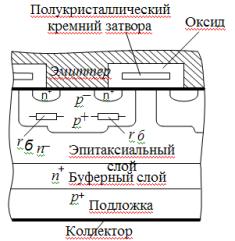
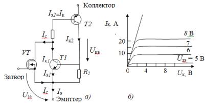
As can be seen from the structure of the IGBT transistor (Fig. 1), it is a rather complex device in which a pn-p transistor is controlled by an n-channel MOS transistor.
The collector of the IGBT transistor (Fig. 2, a) is the emitter of the VT4 transistor. When a positive voltage is applied to the gate, the transistor VT1 has an electrically conducting channel. Through it, the emitter of the IGBT transistor (the collector of the VT4 transistor) is connected to the base of the VT4 transistor.
This leads to the fact that it is completely unlocked and the voltage drop between the collector of the IGBT transistor and its emitter becomes equal to the voltage drop in the emitter junction of the VT4 transistor, summed with the voltage drop Usi across the VT1 transistor.
Due to the fact that the voltage drop in the p — n junction decreases with increasing temperature, the voltage drop in an unlocked IGBT transistor in a certain current range has a negative temperature coefficient, which becomes positive at high current. Therefore, the voltage drop across the IGBT does not fall below the threshold voltage of the diode (VT4 emitter).
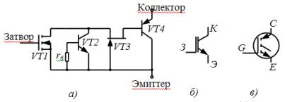
Rice. 2. Equivalent circuit of an IGBT transistor (a) and its symbol in the native (b) and foreign (c) literature
As the voltage applied to the IGBT transistor increases, the channel current increases, which determines the base current of the VT4 transistor, while the voltage drop across the IGBT transistor decreases.
 When the transistor VT1 is locked, the current of the transistor VT4 becomes small, which makes it possible to consider it locked. Additional layers are introduced to disable thyristor-typical modes of operation when an avalanche breakdown occurs. The buffer layer n + and the wide base region n– provide a reduction in the current gain of the p — n — p transistor.
The general picture of switching on and off is quite complex, since there are changes in the mobility of charge carriers, current transfer coefficients in p — n — p and n — p — n transistors present in the structure, changes in the resistances of the regions, etc. . Although in principle IGBT transistors can be used to operate in linear mode, while they are mainly used in key mode.
In this case, the changes in the switch voltages are characterized by the curves shown in Fig.
 Rice. 3. Change in voltage drop Uke and current Ic of the IGBT transistor
Rice. 4. Equivalent diagram of an IGBT type transistor (a) and its current-voltage characteristics (b)
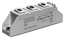
Studies have shown that for most IGBT transistors, the turn-on and turn-off times do not exceed 0.5 — 1.0 μs. To reduce the number of additional external components, diodes are introduced into IGBT transistors or modules consisting of several components are produced (Fig. 5, a — d).
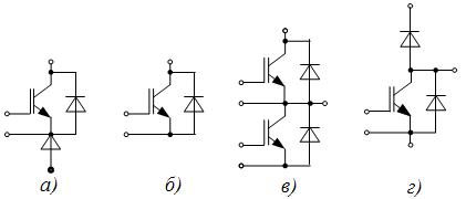
Rice. 5. Symbols of modules of IGBT-transistors: a — MTKID; b — MTKI; c — M2TKI; d — MDTKI
The symbols of IGBT transistors include: letter M — potential-free module (the base is isolated); 2 — the number of keys; letters TCI — bipolar with insulated cover; DTKI — Diode / Bipolar Transistor with Isolated Gate; TCID — Bipolar Transistor / Isolated Gate Diode; numbers: 25, 35, 50, 75, 80, 110, 150 — maximum current; numbers: 1, 2, 5, 6, 10, 12 — the maximum voltage between the collector and the emitter Uke (* 100V). For example, the MTKID-75-17 module has UKE = 1700 V, I = 2 * 75A, UKEotk = 3.5 V, PKmax = 625 W.
Doctor of technical sciences, professor L.A. Potapov