Field effect transistors
 Field-effect (unipolar) transistors are divided into transistors with a control p-n-junction (Fig. 1) and with an isolated gate. The device of a field-effect transistor with a control p-n junction is simpler than a bipolar one.
In an n-channel transistor, the main charge carriers in the channel are electrons that move along the channel from a low-potential source to a higher-potential drain, forming a drain current Ic. A reverse voltage is applied between the gate and source of the FET, which blocks the p-n junction formed by the n-region of the channel and the p-region of the gate.
Thus, in an n-channel FET, the polarities of the applied voltages are as follows: Usi> 0, Usi≤0. When a blocking voltage is applied to the pn junction between the gate and the channel (see Fig. 2, a), a uniform layer, depleted in charge carriers and with high resistance, appears at the channel boundaries.
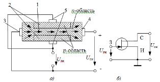
Rice. 1. Structure (a) and circuit (b) of a field-effect transistor with a gate in the form of a p-n junction and an n-type channel; 1,2 — channel and portal zones; 3,4,5 — conclusions of the source, the drain, the prison
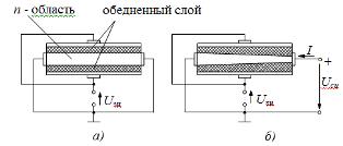
Rice. 2. Channel width in the field-effect transistor at Usi = 0 (a) and at Usi> 0 (b)
This leads to a reduction in the width of the conducting channel. When a voltage is applied between the source and the drain, the depletion layer becomes uneven (Fig. 2, b), the cross-section of the channel near the drain decreases, and the conductivity of the channel also decreases.
The VAH characteristics of the FET are shown in Fig. 3. Here, the dependences of the drain current Ic on the voltage Usi at a constant gate voltage Uzi determine the output or drain characteristics of the field-effect transistor (Fig. 3, a).
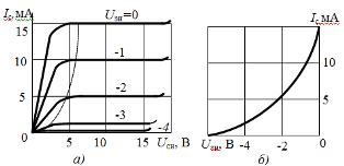
Rice. 3. Output (a) and transfer (b) volt-ampere characteristics of the field-effect transistor.
In the initial section of the characteristics, the drain current increases with increasing Umi. As the source-drain voltage increases to Usi = Uzap– [Uzi], the channel overlaps and further increase in current Ic stops (saturation region).
A negative gate-to-source voltage Uzi results in lower values of the voltage Uc and current Ic where the channel overlaps.
A further increase in the voltage Usi leads to the breakdown of the p — n junction between the gate and the channel and disables the transistor. The output characteristics can be used to construct the transfer characteristic Ic = f (Uz) (Fig. 3, b).
In the saturation section, it is practically independent of the voltage Usi. It shows that in the absence of input voltage (gate - drain), the channel has a certain conductivity and flows a current called the initial drain current Ic0.
In order to effectively "lock" the channel, it is necessary to apply an interrupting voltage Uotc to the input.The input characteristic of the FET — the dependence of the gate drain current I3 on the gate — source voltage — is usually not used, because at Uzi < 0 the p-n junction between the gate and the channel is closed and the gate current is very small (I3 = 10-8 … 10-9 A), so in many cases it can be neglected.
As in this case bipolar transistors, the fields have three switching circuits: with a common gate, drain and source (Fig. 4). The I-V transfer characteristic of a field-effect transistor with a control p-n junction is shown in Fig. 3, b.
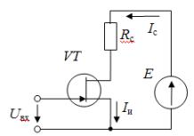
Rice. 4. Switching scheme of a common-source field-effect transistor with a control p-n-junction
The main advantages of field-effect transistors with a control p-n-junction over bipolar ones are high input impedance, low noise, ease of production, low voltage drop in the fully open channel. However, field-effect transistors have such a disadvantage as the need to work in negative regions of I — the V characteristic, which complicates the scheme.
Doctor of technical sciences, professor L.A. Potapov