What is a semiconductor
 Along with the conductors of electricity, there are many substances in nature that have significantly lower electrical conductivity than metal conductors. Substances of this type are called semiconductors.
Semiconductors include: certain chemical elements such as selenium, silicon and germanium, sulfur compounds such as thallium sulfide, cadmium sulfide, silver sulfide, carbides such as carborundum, carbon (diamond), boron, tin, phosphorus, antimony, arsenic, tellurium, iodine, and a number compounds that include at least one of the elements of the 4 — 7 group of the Mendeleev system. There are also organic semiconductors.
The nature of the electrical conductivity of the semiconductor depends on the type of impurities present in the base material of the semiconductor and on the manufacturing technology of its constituent parts.
Semiconductor — substance with electrical conductivity 10-10 — 104 (ohm x cm)-1 located by these properties between the conductor and the insulator.The difference between conductors, semiconductors and insulators according to band theory is as follows: in pure semiconductors and electronic insulators there is a forbidden energy band between the filled (valence) band and the conduction band.
Why semiconductors conduct current
A semiconductor has electronic conductivity if the outer electrons in its impurity atoms are relatively weakly bound to the nuclei of those atoms. If an electric field is created in this type of semiconductor, then under the influence of the forces of this field, the outer electrons of the impurity atoms of the semiconductor will leave the boundaries of their atoms and become free electrons.
The free electrons will create an electrical conduction current in the semiconductor under the influence of the electric field forces. Therefore, the nature of electric current in electrically conducting semiconductors is the same as in metallic conductors. But since there are many times fewer free electrons per unit volume of a semiconductor than per unit volume of a metallic conductor, it is natural that, all other conditions being the same, the current in a semiconductor will be many times smaller than in a metallic conductor.
A semiconductor has "hole" conductivity if the atoms of its impurity not only do not give up their outer electrons, but, on the contrary, tend to capture the electrons of the atoms of the semiconductor's main substance. If an impurity atom takes away an electron from an atom of the main substance, then in the latter is formed a kind of free space for an electron - a "hole".
A semiconductor atom that has lost an electron is called an "electron hole" or simply a "hole".If the "hole" is filled with an electron transferred from a neighboring atom, then it is eliminated and the atom becomes electrically neutral, and the "hole" moves to the neighboring atom that has lost an electron. Therefore, if an electric field is applied to a semiconductor with «hole» conduction, the «electron holes» will move in the direction of this field.
The bias of «Electron holes» in the direction of action of an electric field is similar to the movement of positive electric charges in a field and is therefore a phenomenon of electric current in a semiconductor.
Semiconductors cannot be strictly differentiated according to the mechanism of their electrical conductivity, because along with "Hole" conductivity, this semiconductor can have electronic conductivity to one degree or another.
Semiconductors are characterized by:
-
type of conductivity (electronic - n-type, hole -p -type);
-
resistance;
-
charge carrier lifetime (minority) or diffusion length, surface recombination rate;
-
dislocation density.
See also: Current-voltage characteristics of semiconductors  Silicon is the most common semiconductor material
Temperature has beings that affect the characteristics of semiconductors. Its increase mainly leads to a decrease in resistance and vice versa, i.e. semiconductors are characterized by the presence of negative temperature coefficient of resistance… Near absolute zero, the semiconductor becomes an insulator.
Many devices are based on semiconductors. In most cases, they must be obtained in the form of single crystals.To give the desired properties, semiconductors are doped with various impurities. Increased requirements are imposed on the purity of the starting semiconductor materials.
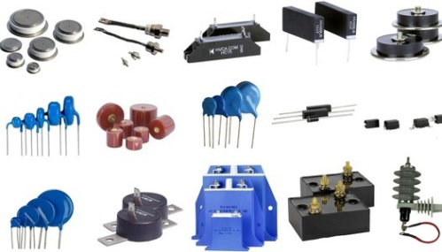
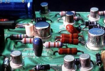
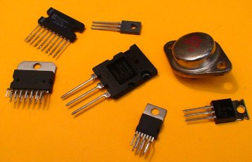 Semiconductor devices
Semiconductor heat treatment
Heat treatment of a semiconductor — heating and cooling of a semiconductor according to a given program in order to change its electrophysical properties.
Changes: crystal modification, dislocation density, concentration of vacancies or structural defects, type of conductivity, concentration, mobility and lifetime of charge carriers. The last four, in addition, can be related to the interaction of impurities and structural defects or to the diffusion of impurities in the bulk of the crystals.
Heating the germanium samples to a temperature >550 °C followed by rapid cooling results in the appearance of thermal acceptors in concentrations the higher the temperature. Subsequent annealing at the same temperature restores the initial resistance.
The probable mechanism of this phenomenon is the dissolution of copper in the germanium lattice that diffuses from the surface or was previously deposited on dislocations. Slow annealing causes copper to deposit on structural defects and exit the grid. The appearance of new structural defects during rapid cooling is also possible. Both mechanisms can reduce the lifetime, which has been established experimentally.
In silicon at temperatures of 350 — 500 °, the formation of thermal donors occurs in concentrations the higher, the more oxygen is dissolved in silicon during crystal growth. At higher temperatures, the heat donors are destroyed.
Heating to temperatures in the range 700 — 1300 ° sharply reduces the lifetime of minority charge carriers (at > 1000 ° the decisive role is played by the diffusion of impurities from the surface). Heating silicon at 1000-1300 ° affects the optical absorption and scattering of light.
Application of semiconductors
In modern technologies, semiconductors have found the widest application; they have had a very strong impact on technological progress. Thanks to them, it is possible to significantly reduce the weight and dimensions of electronic devices. The development of all areas of electronics leads to the creation and improvement of a large number of diverse equipment based on semiconductor devices. Semiconductor devices serve as the basis for microcells, micromodules, hard circuits, etc.
Electronic devices based on semiconductor devices are practically inertialess. A carefully constructed and well-sealed semiconductor device can last for tens of thousands of hours. However, some semiconductor materials have a small temperature limit (for example, germanium), but not very difficult temperature compensation or replacement of the base material of the device with another (for example, silicon, silicon carbide) largely eliminates this drawback. The improvement of semiconductor device manufacturing technology results in a reduction of the still existing parameter dispersion and instability.
 Semiconductors in electronics
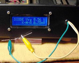
The semiconductor-metal contact and electron-hole junction (n-p junction) created in semiconductors are used in the manufacture of semiconductor diodes.Double junctions (p-n-p or n-R-n) — transistors and thyristors. These devices are mainly used to rectify, generate and amplify electrical signals.
The photoelectric properties of semiconductors are used to create photoresistors, photodiodes, and phototransistors. The semiconductor serves as the active part of the oscillators (amplifiers) of oscillations semiconductor lasers… When an electric current passes through the pn junction in the forward direction, the charge carriers—electrons and holes—recombine with the emission of photons, which is used to create LEDs.
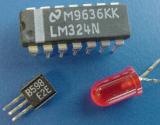
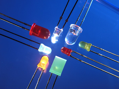 LEDs
LEDs
The thermoelectric properties of semiconductors made it possible to create semiconductor thermoelectric resistances, semiconductor thermocouples, thermocouples and thermoelectric generators and thermoelectric cooling of semiconductors based on the Peltier effect, — thermoelectric refrigerators and thermostabilizers.
Semiconductors are used in mechanical heat and solar energy converters in electrical — thermoelectric generators and photoelectric converters (solar cells).
Mechanical stress applied to a semiconductor changes its electrical resistance (the effect is stronger than for metals), which is the basis of the semiconductor strain gauge.
Semiconductor devices have become widespread in world practice, revolutionizing electronics, they serve as the basis for the development and production of:
-
measuring equipment, computers,
-
equipment for all types of communications and transport,
-
for industrial process automation,
-
research devices,
-
rocket,
-
medical equipment
-
other electronic devices and devices.
The use of semiconductor devices allows you to create new equipment and improve old, which means that it reduces its size, weight, power consumption and, therefore, reducing the generation of heat in the circuit, increasing strength, immediate readiness for action, it gives you allows you to increase the service life and reliability of electronic devices.