Power transistors
The main classes of power transistors
A transistor is a semiconductor device containing two or more pn junctions and capable of operating in both boost and switch modes.
In power electronics, transistors are used as fully controllable switches. Depending on the control signal, the transistor can be closed (low conduction) or open (high conduction).
In the off state, the transistor is able to withstand the forward voltage determined by external circuits, while the transistor current is of small value.
In the open state, the transistor conducts a direct current determined by external circuits, while the voltage between the supply terminals of the transistor is small. Transistors are unable to conduct reverse current and cannot withstand reverse voltage.
According to the principle of operation, the following main classes of power transistors are distinguished:
-
bipolar transistors,
-
field effect transistors, among which the most widespread are metal oxide semiconductor (MOS) transistors (MOSFET — metal oxide semiconductor field effect transistor),
-
field-effect transistors with control p-n-junction or static induction transistors (SIT) (SIT-static induction transistor),
-
insulated gate bipolar transistor (IGBT).
Bipolar transistors
A bipolar transistor is a transistor in which currents are generated by the movement of charges of two characters — electrons and holes.
Bipolar transistors consists of three layers of semiconductor materials with different conductivities. Depending on the order of alternation of the layers of the structure, transistors of pnp and npn types are distinguished. Among power transistors, transistors of the n-p-n type are widespread (Fig. 1, a).
The middle layer of the structure is called the base (B), the outer layer that injects (embeds) carriers is called the emitter (E), and collects the carriers — the collector (C). Each of the layers—base, emitter, and collector—has a wire to connect to circuit elements and external circuits. MOSFET transistors. The principle of operation of MOS transistors is based on a change in the electrical conductivity of the interface between a dielectric and a semiconductor under the influence of an electric field.
From the structure of the transistor, there are the following outputs: gate (G), source (S), drain (D), as well as an output from the substrate (B), usually connected to the source (Fig. 1, b).
The main difference between MOS transistors and bipolar transistors is that they are driven by voltage (the field created by that voltage) rather than current. The main processes in MOS transistors are due to one type of carriers, which increases their speed.
The allowable values of the switched currents of MOS transistors significantly depend on the voltage.At currents up to 50 A, the allowable voltage usually does not exceed 500 V at a switching frequency of up to 100 kHz.
SIT transistors
This is a type of field-effect transistors with a control p-n-junction (Fig. 6.6., C). The operating frequency of SIT transistors usually does not exceed 100 kHz with a switched circuit voltage up to 1200 V and currents up to 200 — 400 A.
IGBT transistors
The desire to combine in one transistor the positive properties of bipolar and field effect transistors led to the creation of the IGBT — transistor (Fig. 1., d).
IGBT — Transistor It has a low turn-on power loss like a bipolar transistor and a high control circuit input impedance typical of a field-effect transistor.
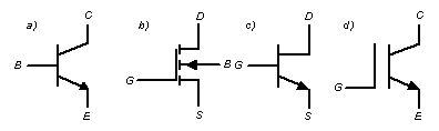
Rice. 1. Conventional graphic designations of transistors: a)-bipolar transistor type p-p-p; b)-MOSFET-transistor with an n-type channel; c)-SIT-transistor with controlling pn-junction; d) — IGBT transistor.
 The switched voltages of power IGBT transistors, as well as bipolar ones, are not more than 1200 V, and the current limit values reach several hundred amperes at a frequency of 20 kHz.
The above characteristics define the areas of application of various types of power transistors in modern power electronic devices. Traditionally, bipolar transistors were used, the main disadvantage of which was the consumption of a significant base current, which required a powerful final control stage and led to a decrease in the efficiency of the device as a whole.
Then field-effect transistors were developed, which are faster and consume less power than the control system.The main disadvantage of MOS transistors is the large loss of power from the flow of the power current, which is determined by the peculiarity of the static I — V characteristic.
Recently, the leading position in the field of application has been occupied by IGBTs — transistors that combine the advantages of bipolar and field-effect transistors. The limiting power of SIT - transistors is relatively small, which is why it is widely used in power electronics they didn't find it.
Ensuring safe operation of power transistors
The main condition for the reliable operation of power transistors is to ensure compliance with the safety operation of both static and dynamic volt-ampere characteristics determined by the specific operating conditions.
The limitations that determine the safety of power transistors are:
-
the maximum allowable current of the collector (drainage);
-
permissible value of the power dissipated by the transistor;
-
the maximum allowable value of the voltage collector — emitter (drain — source);
In the pulse modes of operation of the power transistors, the operational safety limits are significantly extended. This is due to the inertia of thermal processes that cause overheating of the semiconductor structure of the transistors.
The dynamic I — V characteristic of a transistor is largely determined by the parameters of the switched load. For example, switching off an active - inductive load causes an overvoltage on the key element. These overvoltages are determined by the self-inductive EMF Um = -Ldi / dt, which occurs in the inductive component of the load when the current drops to zero.
To eliminate or limit overvoltages during switching of an active - inductive load, various switching path forming (CFT) circuits are used, which enable the desired switching path to be formed. In the simplest case, this can be a diode actively shunting an inductive load, or an RC circuit connected in parallel to the drain and source of the MOS transistor.