Logic gates in electrical circuits
 Logic elements are devices that make a certain connection between input and output values. An elementary logic element has two inputs and one output. The signals to them are discrete, that is, they take one of two possible values - 1 or 0. The presence of voltage is sometimes taken as one, and its absence is sometimes taken as zero. The operation of such devices is analyzed using the concepts of Boolean algebra—algebra of logic.
Devices operating with discrete signals are called discrete. The operation of such devices is analyzed using the concepts of Boolean algebra—algebra of logic.
Fundamentals of Algebra of Logic
A logical variable is an input value that can take only two opposite values: x = 1 or x = 0. A logical function is the dependence of the output value on the input and on the output signal itself, which can also take only two values: y = 1 or y = 0. A logical operation is an action performed by a logical element with logical variables according to a logical function.The values 1 and 0 are mutually opposite (inverted): 1 = 0, 0 = 1. The dash means negation (inversion).
It is assumed that 0 • 0 = 0, 0 + 0 = 0, 1 — 0 = 0, 1 + 0 = 1, 1 • 1 = = 1, 1 + 1 = 1.
When transforming the formulas of logic algebra, inversion operations are performed first, then multiplication, addition, and then all the others.
See also on this topic: Laws of Contact Circuit Algebra
Basic logical operations are discussed here: Logical devices
Logic elements in the form of relay-contact circuits
The logic elements can be represented in the form of a relay-contact circuit (Fig. 1).
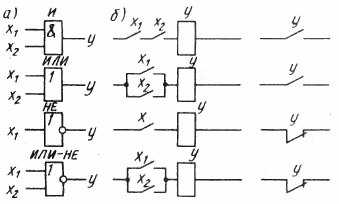
Rice. 1. Basic logic elements (a) and relay contact equivalent (b)
If we assume that closed contacts correspond to one signal and open contacts correspond to zero, then element A can be represented as connected contacts x1 and x2 and relay y. If both contacts are closed, then current will flow through the coil, the relay will operate and its contacts will close.
The OR element can be represented as two NO contacts connected in parallel. When the first or second of them are closed, the relay is activated and closes its contacts through which the signal will pass.
A NOT element can be represented as one NO contact x and one NC contact y. If no signal is applied to the input (x = 0), then the relay does not work and the contacts of y remain closed, current flows through them. If you close the x contacts, the relay will operate and open its contacts, then the output signal will be zero.
In fig. 2 shows a circuit that performs the OR — NOT operation.If no signal is applied to any of the inputs, then the transistor will remain closed, no current will flow through it, and the output voltage will be equal to the source emf Uy = Uc, i.e. y = 1.
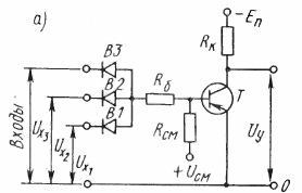
Rice. 2. Scheme of logical element OR — NOT, performing logical operations
If a voltage is applied to at least one of the inputs, then the resistance of the transistor will drop from ∞ to 0 and current will flow through the emitter-collector circuit. The voltage drop across the transistor will be zero (Uy = 0). This means that there is no signal at the output, that is, y = 0. For normal operation of the element, it is necessary to create a displacement of the base potential relative to the common point, this is achieved by a special source Ucm and a resistor Rcm. Resistor R6 limits the base emitter current.
The logic elements built on electromagnetic relays, transistors, magnetic cores, electronic lamp, pneumatic relays are too large, which is why integrated circuits are now used. Logical operations in them are carried out at the crystal level.
Examples of using logic gates in circuits
Let's look at a few electrical circuit assemblies that are most commonly found in an electric drive. In fig. 3a shows the supply unit of the contactor coil K.
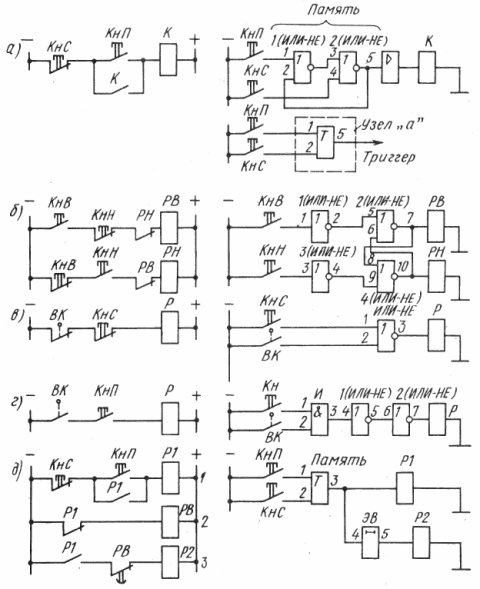
Rice. 3. Circuit nodes with logic elements: 1 — 8 — input and output numbers
When the KNP button is pressed, current flows through the line and the contactor is activated. Its main contacts (not shown in the diagram) connect the motor to the network, and the K contacts, closing, bypass the KNP button. Current will now flow through these contacts and the KNP button can be released.Under the action of the spring, it opens its contacts, but the coil will continue to be energized through the contacts K. When the KnS button is pressed, the line is interrupted and the contactor is released.
This node can be executed on logical elements. The circuit includes the coil of the contactor K, the buttons KNP and KNS, two logic elements OR — NOT and an amplifier. The initial state is x1 = 0 and x2 = 0, then at the output of element 1 we get y1 = x1 + x2 = 0 + 0 = 1. At the output of element 2 — y5 = x3 + x4 = 1 + 0 = 0, t .is the coil is off, the relay is not working.
If you press KnP, then y1 = x1 + x2 = 1 + 0 = 0. At the output of element 2 y5 = x3 + x4 = 0 + 0 = 1. Current flows through the coil and the contactor is activated. The signal y2 is applied to the input x2 but y1 is not changed by this because y1 = x1 + x2 = 1 + 1 = 0. Thus the contactor coil is energized.
If you press the KNS button, then a signal x4 = 1 will be applied to the input of the second element, then y2 = x3 + x4 = 0 + 1 = 0 and the contactor is released.
The circuit under consideration is capable of «memorizing» commands: the signal y2 remains unchanged even if the button is released.
The same memory function can be accomplished with a flip-flop. If a signal x1 = 1 is applied to the input, then the signal y = 1 will appear at the output and will remain unchanged until we press the KnS button. The flip-flop is then switched and a signal y = 0 appears at the output. It will remain unchanged until we press the KNP button again.
In fig. 3, b shows a block for electrical blocking of two relays PB (forward) and PH (reverse), which excludes their simultaneous operation, as this will lead to a short circuit.Indeed, when the KnV button is pressed, the PB relay is activated, and its auxiliary contacts open, and the PH coil cannot be energized even if the KnN button is pressed. Note that there is no maneuvering of the closing contacts of the buttons here, that is, there is no memory module.
In a circuit with logical elements, when we press the KNV button on the first element, we get x1 = 1, y2 = x1 = 0. On the second element, y7 = x5 + x6 = y2 + x6= 0 + 0 = 1
The relay PB is activated and the signal y7 is applied to the input of element 4 (y7 — x8 = 1). There is no signal at the input of element 3 (x2 = 0), then y4 = x2 = 1. On the fourth element: y10 = x8 + x9 = x8 + y4 = 1 + 1 = 0, i.e. the PH relay cannot work , even if the KnN button is pressed. Then we get the same result: 10 = x8 + x9 = = x8 + y4 = 1 + 0 = 0.
In fig. 3, c shows the release relay in case of pressing the button KnS or opening the contacts of the limit switch VK. In a circuit with logic elements in the initial position y3 = x1 + x2 = 0 + 0 = 1, that is, the relay coil is energized. When you press the KnS button, we get y3 = x1 + x2 = 1 + 0 = 0 and the relay is released.
In fig. 3, d shows the device for turning on the relay in case of pressing the KNP button when the VK contact is closed. In a circuit with logic elements in the normal state of the contacts, we get y7 = NS6 = y6 = NS4 = y3 = x1x2 = 0 • 0 = 0. If only the KNP button is pressed, then y7 = x1x2 = 1 • 0 = 0. If only VK contact is closed then y7 = = x1x2 = 0 • 1 = 0 When KNP is closed and VK we get y7 = x1x2 = 1 • 1 = 1. This means the relay is activated.
In fig. 3, e shows a control circuit for two relays P1 and P2.When voltage is applied to the circuit, the time relay PB is activated, its contacts in line 3 open immediately. The circuit is ready for operation. When the KNP button is pressed, relay P1 is activated, its contacts close, bypassing the button. Other contacts on line 2 open and on line 3 close. Relay PB is released and its contacts close with a time delay, relay P2 is activated. Thus, after pressing the KNP button, relay P1 is activated immediately, and P2 - after some time.
In a circuit with logic elements, the "Memory" node is built on a flip-flop. Let there be no signal at the output (y3 = 0), relays P1 and P2 are de-energized. Press the KNP button, a signal appears on the trigger output. Relay P1 is activated and the EV element starts to synchronize.
When signal y5 = 1 occurs, relay P2 is activated. When you press the KnS button, the trigger is switched and then y3 = 0. Relays P1 and P2 are released.
Typical assemblies with logic elements are widely used in more complex circuits, and such circuits are much simpler than relay-contactor equipment circuits.